Pin description – Rainbow Electronics MAX15038 User Manual
Page 9
MAX15038
4A, 2MHz Step-Down Regulator
with Integrated Switches
_______________________________________________________________________________________
9
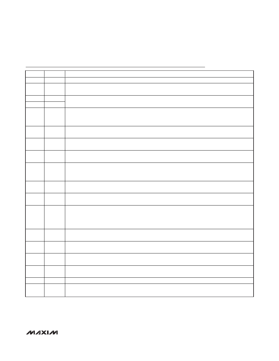
Pin Description
PIN
NAME
FUNCTION
1
MODE
Functional MODE Selection Input. See the MODE Selection section for more information.
2
V
DD
3.3V LDO Output. Supply input for the internal analog core. Connect a low-ESR, ceramic capacitor with a
minimum value of 2.2µF from V
DD
to GND.
3
CTL1
4
CTL2
Preset Output-Voltage Selection Inputs. CTL1 and CTL2 set the output voltage to one of nine preset
voltages. See Table 1 and the Programming the Output Voltage (CTL1, CTL2) section for preset voltages.
5
REFIN
External Reference Input. Connect REFIN to SS to use the internal 0.6V reference. Connecting REFIN to an
external voltage forces FB to regulate to the voltage applied to REFIN. REFIN is internally pulled to GND
when the IC is in shutdown/hiccup mode.
6
SS
Soft-Start Input. Connect a capacitor from SS to GND to set the startup time. Use a capacitor with a 1nF
minimum value. See the Soft-Start and REFIN section for details on setting the soft-start time.
7
GND
Analog Ground Connection. Connect GND and PGND together at one point near the input bypass capacitor
return terminal.
8
COMP
Voltage Error-Amplifier Output. Connect the necessary compensation network from COMP to FB and OUT.
COMP is internally pulled to GND when the IC is in shutdown/hiccup mode.
9
FB
Feedback Input. Connect FB to the center tap of an external resistive divider from the output to GND to set
the output voltage from 0.6V to 90% of V
IN
. Connect FB through an RC network to the output when using
CTL1 and CTL2 to select any of nine preset voltages.
10
OUT
Output-Voltage Sense. Connect to the converter output. Leave OUT unconnected when an external resistive
divider is used.
11
FREQ
Oscillator Frequency Select. Connect a precision resistor from FREQ to GND to select the switching
frequency. See the Frequency Select (FREQ) section.
12
PWRGD
Open-Drain, Power-Good Output. PWRGD is high impedance when V
FB
rises above 92.5% (typ) of V
REFIN
and V
REFIN
is above 0.54V. PWRGD is internally pulled low when V
FB
falls below 90% (typ) of V
REFIN
or
V
REFIN
is below 0.54V. PWRGD is internally pulled low when the IC is in shutdown mode, V
DD
is below the
internal UVLO threshold, or the IC is in thermal shutdown.
13
BST
High-Side MOSFET Driver Supply. Internally connected to IN through a PMOS switch. Bypass BST to LX with
a 0.1µF capacitor.
14, 15,
16
LX
Inductor Connection. All LX pins are internally shorted together. Connect all LX pins to the switched side of
the inductor. LX is high impedance when the IC is in shutdown mode.
17–20
PGND
Power Ground. Connect all PGND pins externally to the power ground plane. Connect all PGND pins
together near the IC.
21, 22,
23
IN
Input Power Supply. Input supply range is from 2.9V to 5.5V. Bypass IN to PGND with a 22µF ceramic
capacitor.
24
EN
Enable Input. Logic input to enable/disable the MAX15038.
—
EP
Exposed Pad. Solder EP to a large contiguous copper plane connected to PGND to optimize thermal
performance. Do not use EP as a ground connection for the device.