Rainbow Electronics MAX15038 User Manual
Page 2
MAX15038
4A, 2MHz Step-Down Regulator
with Integrated Switches
2
_______________________________________________________________________________________
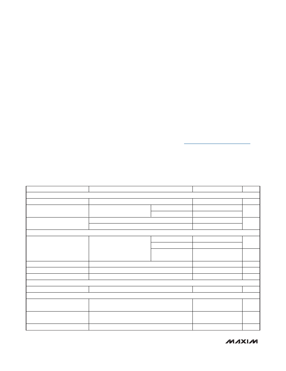
ABSOLUTE MAXIMUM RATINGS
ELECTRICAL CHARACTERISTICS
(V
IN
= V
EN
= 5V, C
VDD
= 2.2µF, T
A
= T
J
= -40°C to +85°C, typical values are at T
A
= +25°C, circuit of Figure 1, unless otherwise
noted.) (Note 3)
Stresses beyond those listed under “Absolute Maximum Ratings” may cause permanent damage to the device. These are stress ratings only, and functional
operation of the device at these or any other conditions beyond those indicated in the operational sections of the specifications is not implied. Exposure to
absolute maximum rating conditions for extended periods may affect device reliability.
IN, PWRGD to GND..................................................-0.3V to +6V
V
DD
to GND ..................-0.3V to the lower of +4V or (V
IN
+ 0.3V)
COMP, FB, MODE, REFIN, CTL1, CTL2, SS,
FREQ to GND ..........................................-0.3V to (V
DD
+ 0.3V)
OUT, EN to GND ......................................................-0.3V to +6V
BST to LX..................................................................-0.3V to +6V
BST to GND ............................................................-0.3V to +12V
PGND to GND .......................................................-0.3V to +0.3V
LX to PGND ..................-0.3V to the lower of +6V or (V
IN
+ 0.3V)
LX to PGND ..........-1V to the lower of +6V or (V
IN
+ 1V) for 50ns
I
LX(RMS)
(Note 1) ......................................................................4A
V
DD
Output Short-Circuit Duration .............................Continuous
Converter Output Short-Circuit Duration ....................Continuous
Continuous Power Dissipation (T
A
= +70°C)
24-Pin TQFN (derate 27.8mW/°C above +70°C) ........2222mW
Thermal Resistance (Note 2)
θ
JA
.................................................................................36°C/W
θ
JC
..................................................................................6°C/W
Operating Temperature Range ...........................-40°C to +85°C
Junction Temperature ......................................................+150°C
Storage Temperature Range .............................-65°C to +150°C
Lead Temperature (soldering, 10s) .................................+300°C
Note 1: LX has internal clamp diodes to PGND and IN. Applications that forward bias these diodes should take care not to exceed
the IC’s package power dissipation limits.
Note 2: Package thermal resistances were obtained using the method described in JEDEC specification JESD51-7, using a four-
layer board. For detailed information on package thermal considerations, refer to
www.maxim-ic.com/thermal-tutorial
.
PARAMETER
CONDITIONS
MIN
TYP
MAX
UNITS
IN
IN Voltage Range
2.9
5.5
V
V
IN
= 3.3V
4.7
8
IN Supply Current
f
S
= 1MHz, no load
V
IN
= 5V
5
8.5
mA
V
IN
= 5V, V
EN
= 0
10
20
Total Shutdown Current from IN
V
IN
= V
DD
= 3.3V, V
EN
= 0
45
µA
3.3V LDO (V
DD
)
V
DD
rising
2.6
2.8
V
DD
falling
2.35
2.55
V
V
DD
Undervoltage Lockout
Threshold
LX starts/stops switching
Minimum glitch-width
rejection
10
µs
V
DD
Output Voltage
V
IN
= 5V, I
VDD
= 0 to 10mA
3.1
3.3
3.5
V
V
DD
Dropout
V
IN
= 2.9V, I
VDD
= 10mA
0.08
V
V
DD
Current Limit
V
IN
= 5V, V
DD
= 0
25
40
mA
BST
BST Supply Current
V
BST
= V
IN
= 5V, V
LX
= 0 or 5V, V
EN
= 0
0.025
µA
PWM COMPARATOR
PWM Comparator Propagation
Delay
10mV overdrive
20
ns
PWM Peak-to-Peak Ramp
Amplitude
1
V
PWM Valley Amplitude
0.8
V