Rainbow Electronics MAX15038 User Manual
Page 15

MAX15038
The high switching frequency range of the MAX15038
allows the use of ceramic output capacitors. Since the
ESR of ceramic capacitors is typically very low, the fre-
quency of the associated transfer function zero is higher
than the unity-gain crossover frequency, fC, and the zero
cannot be used to compensate for the double pole creat-
ed by the output filtering inductor and capacitor. The dou-
ble pole produces a gain drop of 40dB/decade and a
phase shift of 180°. The compensation network error
amplifier must compensate for this gain drop and phase
shift to achieve a stable high-bandwidth closed-loop sys-
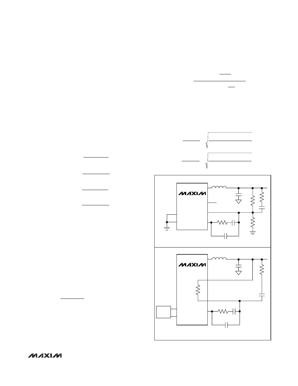
tem. Therefore, use type III compensation as shown in
Figures 3 and 4. Type III compensation possesses three
poles and two zeros with the first pole, fP1_EA, located at
zero frequency (DC). Locations of other poles and zeros
of the type III compensation are given by:
The above equations are based on the assumptions
that C1 >> C2, and R3 >> R2, which are true in most
applications. Placements of these poles and zeros are
determined by the frequencies of the double pole and
ESR zero of the power transfer function. It is also a
function of the desired close-loop bandwidth. The fol-
lowing section outlines the step-by-step design proce-
dure to calculate the required compensation
components for the MAX15038. When the output volt-
age of the MAX15038 is programmed to a preset volt-
age, R3 is internal to the IC and R4 does not exist
(Figure 3b).
When externally programming the MAX15038 (Figure
3a), the output voltage is determined by:
For a 0.6V output, connect an 80k
Ω resistor from FB to
OUT. The zero-cross frequency of the close-loop, f
C
should be between 10% and 20% of the switching fre-
quency, f
S
. A higher zero-cross frequency results in
faster transient response. Once f
C
is chosen, C1 is cal-
culated from the following equation:
where V
P-P
is the ramp peak-to-peak voltage (1V typ).
Due to the underdamped nature of the output LC double
pole, set the two zero frequencies of the type III compen-
sation less than the LC double-pole frequency to provide
adequate phase boost. Set the two zero frequencies to
80% of the LC double-pole frequency. Hence:
C
x R
x
L x C
x R
ESR
R
R
O
O
L
O
3
1
0 8
3
=
+
+
.
(
)
R
x C
x
L x C
x R
ESR
R
R
O
O
L
O
1
1
0 8
1
=
+
+
.
(
)
C
x
V
V
x
x R x
R
R
f
IN
P P
L
O
C
1
2 5
2
3
1
=
+
×
−
.
(
)
π
R
R
V
for V
V
OUT
OUT
4
0 6
3
0 6
0 6
=
×
−
>
.
(
. )
(
.
)
f
R
C
P
EA
2
1
2
2
3
_
=
Ч
Ч
π
f
R
C
P
EA
3
1
2
1
2
_
=
Ч
Ч
π
f
R
C
Z
EA
2
1
2
3
3
_
=
Ч
Ч
π
f
R
C
Z
EA
1
1
2
1
1
_
=
Ч
Ч
π
4A, 2MHz Step-Down Regulator
with Integrated Switches
______________________________________________________________________________________
15
MAX15038
L
C
OUT
EXTERNAL RESISTIVE DIVIDER
INTERNAL PRESET VOLTAGES
V
OUT
R3
R4
R1
COMP
FB
OUT
CTL1
CTL2
LX
C1
C3
R2
C3
R2
C2
MAX15038
L
a)
b)
C
OUT
V
OUT
R3
8k
Ω
R1
COMP
OUT
FB
CTL1
VOLTAGE
SELECT
CTL2
LX
C1
C2
Figure 3. Type III Compensation Network
