Electrical characteristics (continued) – Rainbow Electronics MAX8621Z User Manual
Page 5

MAX8621Y/MAX8621Z
Dual Step-Down DC-DC Power-Management ICs
for Portable Devices
_______________________________________________________________________________________
5
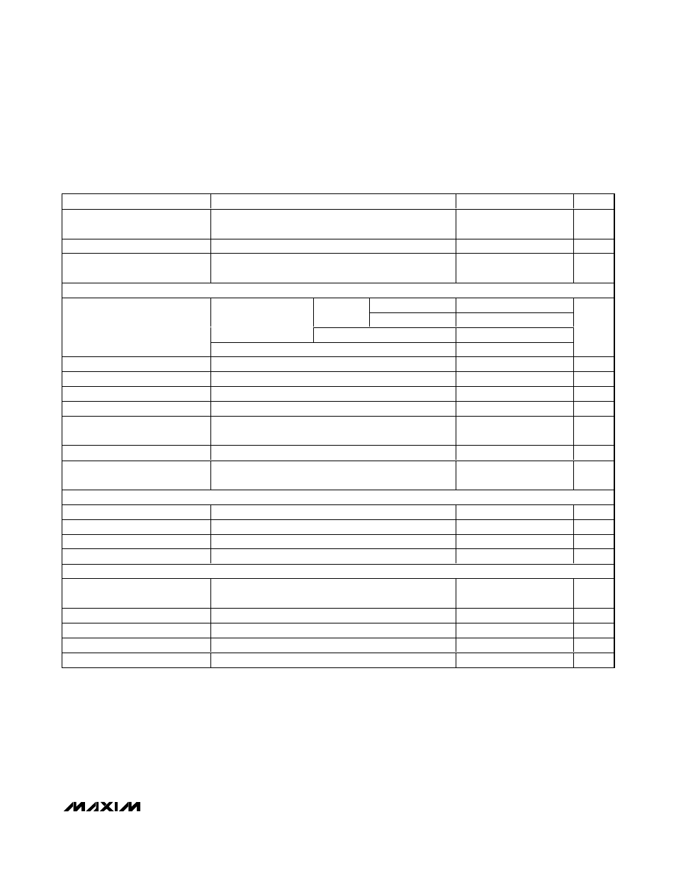
ELECTRICAL CHARACTERISTICS (continued)
(V
IN
= 3.7V, C
IN1
= 10µF, C
IN2
= C
IN3
= 4.7µF, C
OUT1
= C
OUT2
= 4.7µF, C
OUT3
= C
OUT4
= 2.2µF, C
REFBP
= 0.01µF, T
A
= -40°C to
+85°C, unless otherwise noted. Typical values are at T
A
= +25°C.) (Notes 1, 2)
PARAMETER
CONDITIONS
MIN
TYP
MAX
UNIT
Power-Supply Rejection
∆V
OUT3
/
∆V
IN2
10Hz to 10kHz, C
OUT3
= 2.2µF, I
LOAD
= 30mA
60
dB
Output Noise Voltage (RMS)
100Hz to 100kHz, C
OUT3
= 2.2µF, I
LOAD
= 30mA
45
µV
RMS
Output Capacitor for Stable
Operation
0 < I
LOAD
< 150mA
2.2
µF
OUT4 (LDO4)
V
OUT(NOM)
≥ 1.8V
-1.3
+0.3
+2.0
T
A
= 0°C to
+85°C
V
OUT(NOM)
= 1.5V
-1.30
+0.3
+2.35
I
LOAD
= 1mA, 3.7V
≤
V
IN_
≤ 5.5V, relative to
V
OUT(NOM)
T
A
= -40°C to +85°C
-2.3
+2.5
Output Voltage Accuracy
I
LOAD
= 75mA, relative to V
OUT(NOM)
0
%
Output Current
150
mA
Current Limit
V
OUT4
= 0V
165
360
650
mA
Dropout Voltage
I
LOAD
= 100mA, T
A
= +85°C
100
210
mV
Load Regulation
1mA < I
LOAD
< 150mA, V
SEL1
= V
SEL2
= 0
0.6
%
Power-Supply Rejection
∆V
OUT4
/
∆V
IN2
10Hz to 10kHz, C
OUT4
= 2.2µF, I
LOAD
= 30mA
60
dB
Output Noise Voltage (RMS)
100Hz to 100kHz, C
OUT4
= 2.2µF, I
LOAD
= 30mA
45
µV
RMS
Output Capacitor for Stable
Operation
0 < I
LOAD
< 150mA
2.2
µF
DRIVER (DR)
ENDR Turn-On Threshold
I
DR
= 1mA
0.65
V
ENDR Input Current
V
ENDR
= 0V and 5.5V
-1
+1
µA
DR Output Low Voltage
I
DR
= 150mA, V
ENDR
= 3.7V
0.2
0.4
V
DR Off-Current (Leakage)
V
DR
= V
IN
= 5.5V, V
ENDR
= 0V
-1
+1
µA
RESET
Output High Voltage
V
OUT1
- 0.3V
V
Output Low Voltage
I
SINK
= 1mA
0.3
V
RESET Threshold
Percentage of nominal OUT1 rising when RESET falls
84
87
90
%
RESET Active Timeout Period
From OUT1
≥ 87% until RESET = HIGH
60
ms
Pullup Resistance to OUT1
8
14
20
k
Ω
Note 1: V
IN1
, V
IN2
, and V
IN3
are shorted together and single input is referred to as V
IN
.
Note 2: All units are 100% production tested at T
A
= +85°C. Limits over the operating range are guaranteed by design.
Note 3: OUT1, OUT2, OUT3, OUT4, LX1, and LX2 to ground.
Note 4: When the input voltage is greater than 2.85V (typ), the UVLO comparator trips and the threshold is reduced to 2.35V (typ).
This allows the system to start normally until the input voltage decays to 2.35V.
