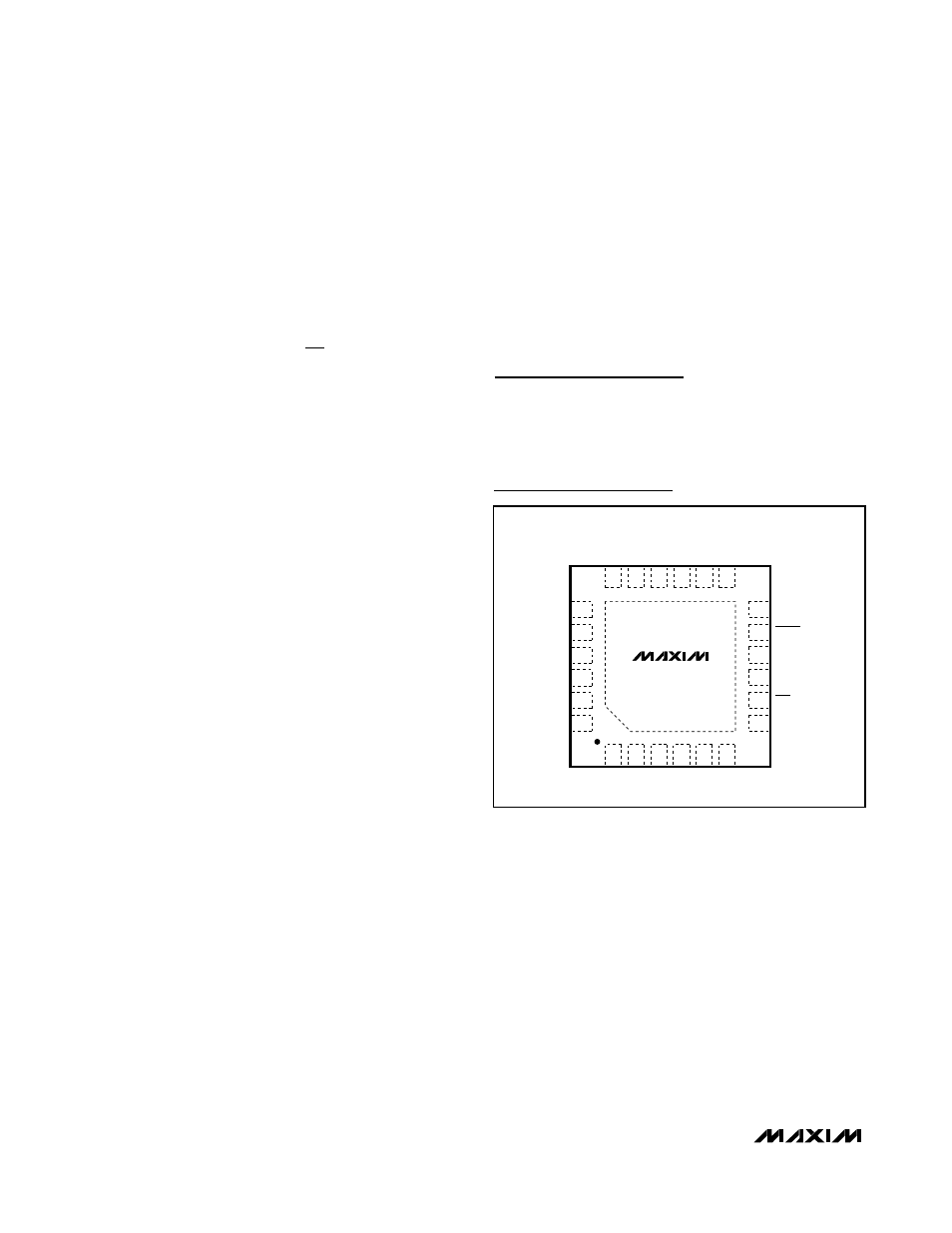
Pin configuration, Chip information – Rainbow Electronics MAX8621Z User Manual
Page 16

The die junction temperature can be calculated as follows:
When operating at an ambient temp of +70°C under the
above conditions:
T
J
should not exceed +150°C in normal operating con-
ditions.
Printed Circuit Board Layout and Routing
High switching frequencies and relatively large peak
currents make the PC board layout a very important
aspect of design. Good design minimizes excessive
EMI on the feedback paths and voltage gradients in the
ground plane, both of which can result in instability or
regulation errors. Connect C
IN_
close to IN_ and GND.
Connect the inductor and output capacitors (C
OUT_
) as
close to the IC as possible and keep the traces short,
direct, and wide.
The traces between C
OUT_
, C
FF_
, and FB_ are sensitive
to inductor magnetic field interference. Route these
traces between ground planes or keep the traces away
from the inductors.
Connect GND and PGND_ to the ground plane. The
external feedback network should be very close to the
FB pin, within 0.2in (5mm). Keep noisy traces, such as
the LX node, as short as possible. Connect GND to the
exposed paddle directly under the IC. Refer to the
MAX8621Y/MAX8621Z evaluation kit for an example PC
board layout and routing.
T
C
W
C
W
C
J
=
° +
°
⎛
⎝⎜
⎞
⎠⎟
=
°
70
1 182
36
112 6
.
.
T
T
P
J
A
D
JA
=
+
× θ
MAX8621Y/MAX8621Z
Dual Step-Down DC-DC Power-Management ICs
for Portable Devices
16
______________________________________________________________________________________
Pin Configuration
MAX8621Y
MAX8621Z
1
5
4
3
2
FB2
REFBP
6
7
10
9
8
11
12
13
14
15
16
17
18
21
20
19
24
23
22
FB1
GND
OUT4
EN4
OUT2
OUT1
IN2
EN3
PGND2
IN1
DR
LX2
PGND1
LX1
SEL2
ENDR
SEL1
IN3
OUT3
PWRON
RESET
EN2
TOP VIEW
Chip Information
TRANSISTOR COUNT: 5850
PROCESS: BiCMOS
