Pin description, Detailed description – Rainbow Electronics MAX5102 User Manual
Page 6
MAX5102
+2.7V to +5.5V, Low-Power, Dual, Parallel
8-Bit DAC with Rail-to-Rail Voltage Outputs
6
_______________________________________________________________________________________
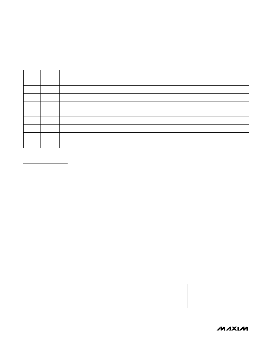
Pin Description
DAC A Voltage Output
OUTA
16
Data Inputs
D7–D0
5–12
DAC Address Select Bit
A0
13
Ground
GND
14
DAC B Voltage Output
OUTB
15
Write Input (active low). Use WR to load data into the DAC input latch selected by A0.
WR
4
Shutdown. Connect SHDN to GND for normal operation.
SHDN
3
PIN
Reference Voltage Input
REF
2
Positive Supply Voltage. Bypass V
DD
to GND using a 0.1µF capacitor.
V
DD
1
FUNCTION
NAME
Detailed Description
Digital-to-Analog Section
The MAX5102 uses a matrix decoding architecture for the
DACs. The external reference voltage is divided down by
a resistor string placed in a matrix fashion. Row and col-
umn decoders select the appropriate tab from the resistor
string to provide the needed analog voltages. The resistor
network converts the 8-bit digital input into an equivalent
analog output voltage in proportion to the applied refer-
ence voltage input. The resistor string presents a code-
independent input impedance to the reference and
guarantees a monotonic output.
These devices can be used in multiplying applications.
Their voltages are buffered by rail-to-rail op amps con-
nected in a follower configuration to provide a rail-to-rail
output (see Functional Diagram).
Low-Power Shutdown Mode
The MAX5102 features a shutdown mode that reduces
current consumption to 1nA. A high voltage on the
SHDN pin shuts down the DACs and the output ampli-
fiers. In shutdown mode, the output amplifiers enter a
high-impedance state. When bringing the device out of
shutdown, allow 13µs for the output to stabilize.
Output Buffer Amplifiers
The DAC outputs are internally buffered by precision
amplifiers with a typical slew rate of 0.6V/µs. The typical
settling time to ±1/2LSB at the output is 6µs when
loaded with 10k
Ω in parallel with 100pF.
Reference Input
The MAX5102 provides a code-independent input
impedance on the REF input. Input impedance is typi-
cally 460k
Ω in parallel with 15pF, and the reference
input voltage range is 0 to V
DD
. The reference input
accepts positive DC signals, as well as AC signals with
peak values between 0 and V
DD
. The voltage at REF
sets the full-scale output voltage for the DAC. The out-
put voltage (V
OUT
) for any DAC is represented by a
digitally programmable voltage source as follows:
V
OUT
= (N
B
· V
REF
) / 256
where N
B
is the numeric value of the DAC binary input
code.
Digital Inputs and Interface Logic
In the MAX5102, address line A0 selects the DAC that
receives data from D0–D7, as shown in Table 1. When
WR is low, the addressed DAC’s input latch is transpar-
ent. Data is latched when WR is high. The DAC outputs
(OUTA, OUTB) represent the data held in the two 8-bit
WR
H
L
LATCH STATE
Input data latched
L
X
A0
DAC A input latch transparent
L
H
DAC B input latch transparent
Table 1. MAX5102 Addressing Table
(partial list)
H = High state, L = Low state, X = Don’t care