Electrical characteristics (continued) – Rainbow Electronics MAX5102 User Manual
Page 3
MAX5102
+2.7V to +5.5V, Low-Power, Dual, Parallel
8-Bit DAC with Rail-to-Rail Voltage Outputs
_______________________________________________________________________________________
3
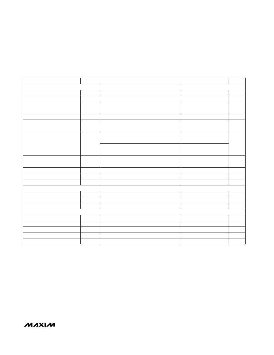
Note 1: Reduced digital code range (code 00 hex to code F0 hex) due to swing limitations when the output amplifier is loaded.
Note 2: Gain error is: [100 (V
F0,meas
- ZCE - V
F0,ideal
) / V
REF
]. Where V
F0,meas
is the DAC output voltage with input code F0 hex,
and V
F0,ideal
is the ideal DAC output voltage with input code F0 hex (i.e., V
REF
·
240 / 256).
Note 3: Output settling time is measured from the 50% point of the falling edge of WR to ±1/2LSB of V
OUT
’s final value.
Note 4: Channel-to-channel isolation is defined as the glitch energy at a DAC output in response to a full-scale step change on any
other DAC output. The measured channel has a fixed code of 80 hex.
Note 5: Digital feedthrough is defined as the glitch energy at any DAC output in response to a full-scale step change on all eight
data inputs with WR at V
DD
.
Note 6: R
L
=
∞, digital inputs at GND or V
DD
.
Note 7: Timing measurement reference level is (V
IH
+ V
IL
) / 2.
ELECTRICAL CHARACTERISTICS (continued)
(V
DD
= V
REF
= +2.7V to +5.5V, GND = 0V, R
L
= 10k
Ω, C
L
= 100pF, T
A
= T
MIN
to T
MAX
, unless otherwise noted. Typical values are at
V
DD
= V
REF
= +3V and T
A
= +25°C.)
60
CONDITIONS
UNITS
MIN
TYP
MAX
SYMBOL
PARAMETER
From code 00 to code F0 hex
REF = 0.5Vp-p, V
REF(DC)
= 1.5V,
V
DD
= 3V, -3dB bandwidth
To 1/2LSB, from code 00 to code F0 hex
Code 00 to code FF hex
Code 00 to code FF hex
I
DD
< 5µA
Code 80 hex to code 7F hex
To ±1/2LSB of final value of V
OUT
ns
20
t
WR
WR Pulse Width
ns
0
t
DH
Data to WR Hold
ns
25
t
DS
Data to WR Setup
ns
0
t
AH
Address to WR Hold
ns
5
t
AS
Address to WR Setup
µA
0.001
1
Shutdown Current
µA
190
360
I
DD
Supply Current (Note 6)
V
2.7
5.5
V
DD
Power-Supply Voltage
µs
20
t
SDN
Time to Shutdown
µs
13
t
SDR
Shutdown Recovery Time
V/µs
0.6
Output Voltage Slew Rate
µV
RMS
60
Wideband Amplifier Noise
kHz
650
Multiplying Bandwidth
70
µs
6
Output Settling Time (Note 3)
nVs
500
Channel-to-Channel Isolation
(Note 4)
nVs
0.5
Digital Feedthrough (Note 5)
nVs
90
Digital-to-Analog Glitch Impulse
REF = 2.5Vp-p at 1kHz, V
REF(DC)
= 1.5V,
V
DD
= 3V, code FF hex
Signal-to-Noise plus Distortion
Ratio
SINAD
dB
REF = 2.5Vp-p at 10kHz, V
REF(DC)
= 1.5V,
V
DD
= 3V, code FF hex
DYNAMIC PERFORMANCE
POWER SUPPLIES
DIGITAL TIMING (Figure 1) (Note 7)