Applications information – Rainbow Electronics MAX4884 User Manual
Page 9
Current-Limit Switch
When the forward- or reverse-current-limit threshold is
exceeded, t
BLANK
timer begins counting. The timer
resets if the overcurrent condition disappears before
t
BLANK
has elapsed. The internal switch is latched off if
the overcurrent condition continues up to the end of the
blanking time (MAX4881/MAX4882/MAX4883B/
MAX4884B). The MAX4883C/MAX4884C limit the cur-
rent infinitely until the thermal trip point occurs. Reset
the switch by toggling EN or CB or IN (Figure 6).
EN
Input
The MAX4881–MAX4884 feature an active-low enable
input (EN). Drive EN low or connect to ground for nor-
mal operation. Drive EN high to force the external n-
channel MOSFET off, and to disable OV and FLAGI.
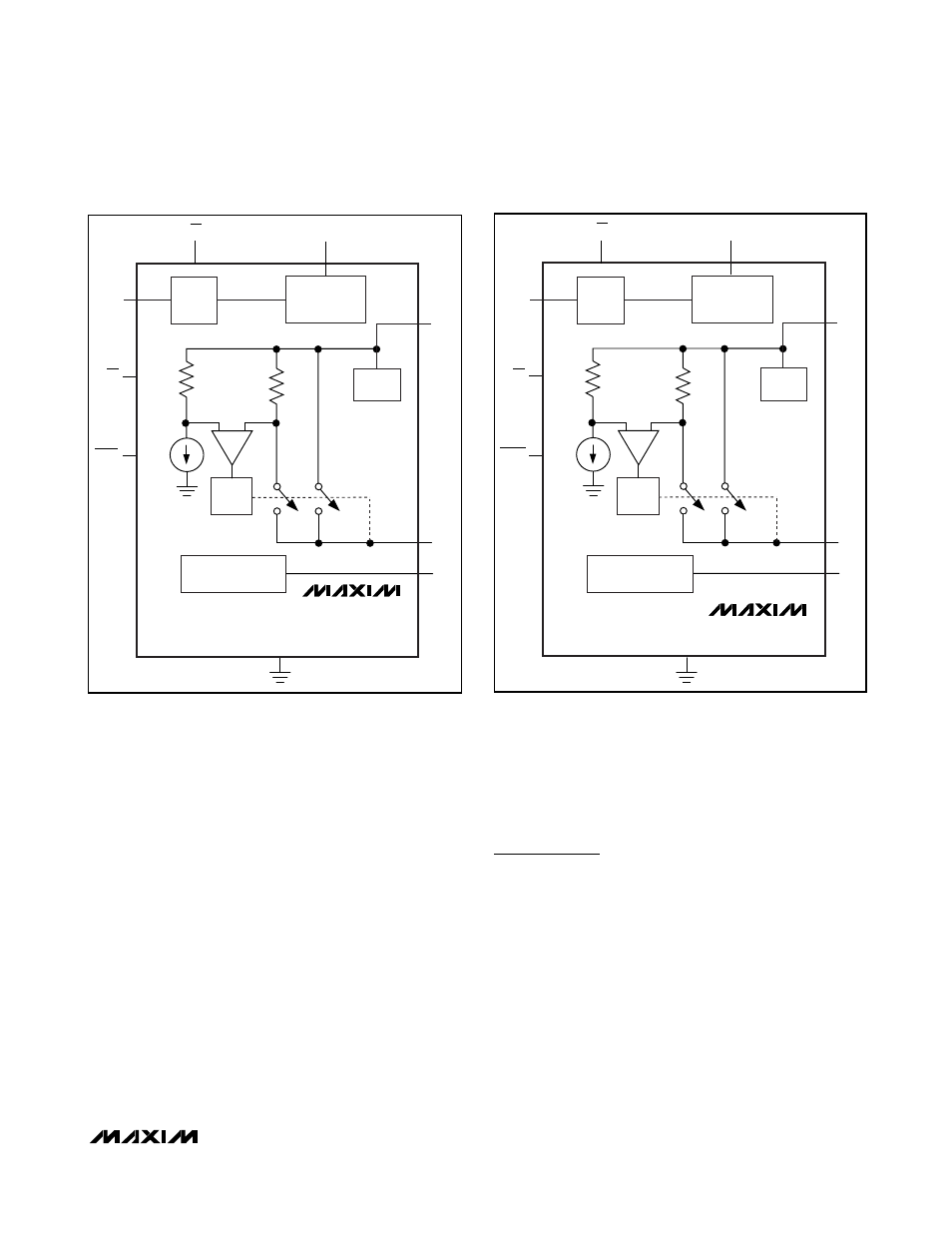
GATE Driver
An on-chip charge pump drives the GATE voltage to
about twice above V
IN
, allowing the use of a low-cost n-
channel MOSFET (
Figure 7). The actual GATE output
voltage tracks approximately 2 x V
IN
until V
IN
exceeds
the OVLO trip level, 5.6V (MAX4881/MAX4883) and
4.5V (MAX4882/MAX4884) typically. The GATE output
voltage, as a function of input voltage, is shown in the
Typical Operating Characteristics.
Applications Information
MOSFET Selection
The MAX4881–MAX4884 are designed for use with
an n-channel MOSFET. MOSFETs with R
DS(ON)
, speci-
fied for a V
GS
of 4.5V or less, work well. If the input sup-
ply is near the UVLO minimum of 4.2V (MAX4881/
MAX4883), or of 2.4V (MAX4882/MAX4884), consider
using a MOSFET specified for a lower V
GS
voltage. Also,
the V
DS
should be 30V for the MOSFET to withstand the
full 28V IN range of the MAX4881–MAX4884. Table 1
shows a selection of MOSFETs appropriate for use with
the MAX4881–MAX4884.
IN Bypass Considerations
Bypass IN to GND with a 1µF ceramic capacitor to
achieve 15kV ESD-protected input. When the power
MAX4881–MAX4884
Overvoltage Protection Controllers with
Current Limit in TDFN
_______________________________________________________________________________________
9
IN
OVLO
UVLO
CHARGE PUMP
IN
OV
FLAGI
EN
CHARGE
PUMP
GND
1.1A/0.7A
LIMIT
I
REF
BTA
UVLO
BTA
BTB
CB
MAX4881/MAX4882
MAX4883B/MAX4884B
BLANKING TIME
AND LATCH-OFF LOGIC
GATE
Figure 7a. MAX4881/MAX4882/MAX4883B/MAX4884B
Functional Diagram
IN
OVLO
UVLO
CHARGE PUMP
GATE
IN
OV
FLAGI
EN
CHARGE
PUMP
GND
1.1A/0.7A
LIMIT
I
REF
BTA
UVLO
BTA
BTB
CB
MAX4883C/MAX4884C
BLANKING TIME
LOGIC
Figure 7b. MAX4883C/MAX4884C Functional Diagram