Detailed description – Rainbow Electronics MAX4884 User Manual
Page 7

Detailed Description
The MAX4881–MAX4884 provide up to +28V overvolt-
age protection for low-voltage systems. When the input
voltage at IN exceeds the overvoltage trip level (OVLO),
the MAX4881–MAX4884 turn off the low-cost external n-
channel FET to prevent damage to the protected compo-
nents and issue an overvoltage fault flag.
The MAX4881–MAX4884 feature a built-in current-limited
switch that limits the load current to 1.1A (MAX4881/
MAX4882) and 0.7A (MAX4883B/MAX4883C/MAX4884B/
MAX4884C). When the load current is at the current limit
for longer than the blanking time, the switch of the
MAX4881/MAX4882/MAX4883B/MAX4884B latches off
and does not turn back on until EN or CB or IN is cycled.
A current-limit flag (FLAGI) asserts to indicate a current
fault condition. The MAX4883C/MAX4884C limit the cur-
rent to 0.7A indefinitely until the thermal protection trips.
An overcurrent flag output asserts to indicate a current
fault condition after the blanking time has elapsed.
IN-Undervoltage Lockout (UVLO)
The MAX4881/MAX4883 have a fixed 4.35V undervolt-
age lockout level (UVLO) while the MAX4882/MAX4884
have a fixed UVLO of 2.55V. GATE goes low when V
IN
is below V
UVLO
, turning off the external n-channel FET.
IN-Overvoltage Lockout (OVLO)
The MAX4881/MAX4883 have a fixed 5.6V overvoltage
threshold (OVLO), while the MAX4882/MAX4884 have a
fixed OVLO of 4.5V. GATE goes low when V
IN
is higher
than V
OVLO
, turning off the external n-channel FET.
Fault Flag Output (
OV
)
The OV output signals the host system that there is a fault
with the input voltage. OV asserts low in response to
either an overvoltage or undervoltage fault. OV stays low
for 50ms after GATE turns on, before deasserting high.
OV is an open-drain active-low output. Connect a
pullup resistor from OV to the logic I/O voltage of the
host system, or to any voltage source up to 6V. Driving
EN high disables OV.
MAX4881–MAX4884
Overvoltage Protection Controllers with
Current Limit in TDFN
_______________________________________________________________________________________
7
V
IN
1.2V
V
GATE
V
UVLO
0.3V
t
START
2.4V
t
0V-BLANK
8V
t
GON
V
OV
5V
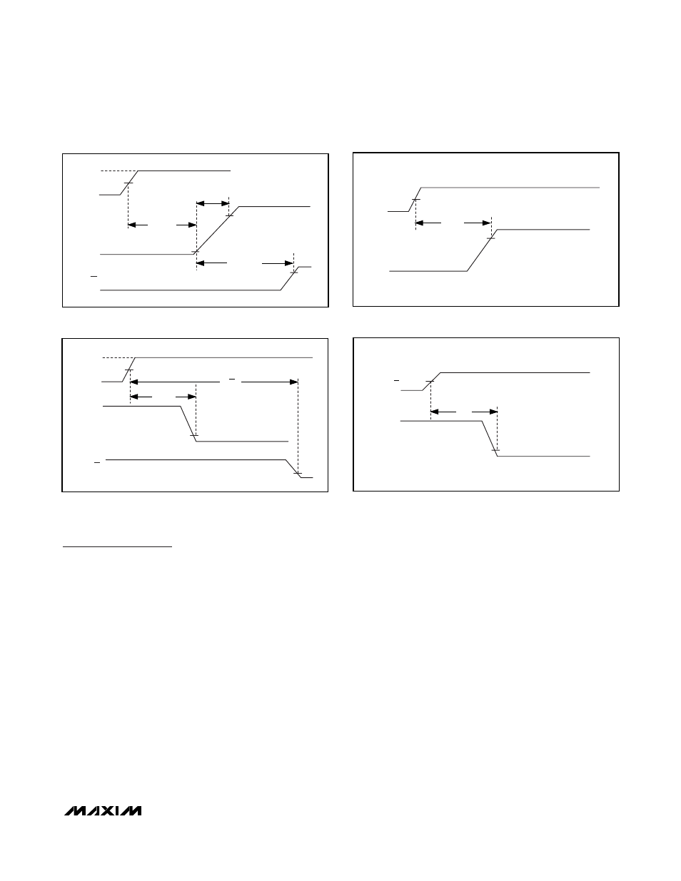
Figure 1. Startup Timing Diagram
V
IN
V
GATE
V
OVLO
0.3V
t
GOFF
0.4V
t
OV
4V/5V
7V/8V
V
OV
Figure 2. Shutdown Timing Diagram
V
IN
I
GATE
V
OVLO
80%
t
OVP
0V
Figure 3. Power-Up Overvoltage Timing Diagram
V
GATE
0.3V
t
DIS
2.4V
V
EN
Figure 4. Disable Timing Diagram
