Application information – Rainbow Electronics ADC08062 User Manual
Page 14
Application Information
(Continued)
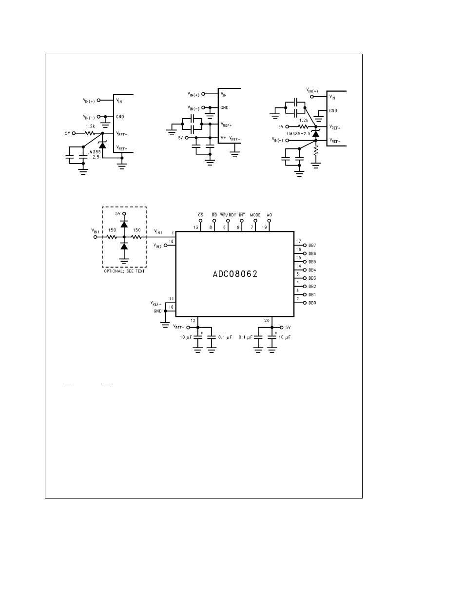
External Reference 2 5V Full-Scale
(Standard Application)
TL H 11086 – 20
Power Supply as Reference
TL H 11086 – 21
Input Not Referred to GND
TL H 11086 – 22
Signal source driving V
IN
(
b
) must be capable of
sinking 5 mA
Note
Bypass capacitors consist of a 0 1 mF ceramic in parallel with a 10 mF bead tantalum
FIGURE 7 Analog Input Options
TL H 11086 – 23
Note the multiple bypass capacitors on the reference and power supply pins V
REF
b
should be bypass to analog ground using multiple capacitors if it is not
grounded (see Section 7 0 ‘‘Layout Grounds and Bypassing’’) V
IN1
is shown with an optional input protection network
FIGURE 8 Typical Connection
the WR signal The WR input signal allows the A D to be
synchronized to a DSP system’s sampling rate or to other
ADC08061 and ADC08062s
The ADC08061 can perform accurate conversions of full-
scale input signals at frequencies from dc to more than
300 kHz (full power bandwidth) without the need of an exter-
nal sample-and-hold (S H)
7 0 LAYOUT GROUNDS AND BYPASSING
In order to ensure fast accurate conversions from the
ADC08061 2 it is necessary to use appropriate circuit
board layout techniques Ideally the analog-to-digital con-
verter’s ground reference should be low impedance and
free of noise from other parts of the system Digital circuits
can produce a great deal of noise on their ground returns
and therefore should have their own separate ground lines
Best performance is obtained using separate ground planes
for the digital and analog parts of the system
The analog inputs should be isolated from noisy signal
traces to avoid having spurious signals couple to the input
Any external component (e g an input filter capacitor) con-
nected across the inputs should be returned to a very clean
ground point Incorrectly grounding the ADC08061 2 will re-
sult in reduced conversion accuracy
The V
a
supply pin V
REF
a
and V
REF
b
(if not grounded)
should be bypassed with a parallel combination of a 0 1 mF
ceramic capacitor and a 10 mF tantalum capacitor placed as
close as possible to the supply pin using short circuit board
traces See
Figures 7
and
8
http
www national com
14