Pin description – Rainbow Electronics ADC08062 User Manual
Page 10
Pin Description
V
IN
V
IN1 – 8
These are analog inputs The input range is
GND – 50 mV
s
V
INPUT
s
V
a
a
50 mV The
ADC08061 has a single input (V
IN
) and the
ADC08062 has a two-channel multiplexer
(V
IN1 – 2
)
DB0 – DB7
TRI-STATE data outputs
bit 0 (LSB) through
bit 7 (MSB)
WR RDY
WR-RD Mode
(Logic high applied to MODE
pin)
WR
With CS low the conversion is started on
the falling edge of WR The digital result will be
strobed into the output latch at the end of con-
version (see
Figures 2a 2b
and
3
)
RD Mode
(Logic low applied to MODE pin)
RDY
This is an open drain output (no internal
pull-up device) RDY will go low after the falling
edge of CS and return high at the end of con-
version
Mode
Mode (RD or WR-RD) selection input
MODE
This pin is pulled to a logic low through an inter-
nal 50 mA current sink when left unconnected
RD Mode
is selected if the MODE pin is left
unconnected or externally forced low A com-
plete conversion is accomplished by pulling RD
low until output data appears
WR-RD Mode
is selected when a high is ap-
plied to the MODE pin A conversion starts with
the WR signal’s rising edge and then using RD
to access the data
WR-RD Mode
(logic high on the MODE pin)
RD
This is the active low Read input With a logic
low applied to the CS pin the TRI-STATE data
outputs (DB0 – DB7) will be activated when RD
goes low (see
Figures 2a 2b
and
3
)
RD Mode
(logic low on the MODE pin)
With CS low a conversion starts on the falling
edge of RD Output data appears on DB0 – DB7
at the end of conversion (see
Figures 1
and
4
)
INT
This is an active low output that indicates that a
conversion is complete and the data is in the
output latch INT is reset by the rising edge of
RD
GND
This is the power supply ground pin
The
ground pin should be connected to a ‘‘clean’’
ground reference point
V
REF
b
These are the reference voltage inputs They
V
REF
a
may be placed at any voltage between GND b
50 mV and V
a
a
50 mV but V
REF
a
must be
greater than V
REF
b
Ideally an input voltage
equal to V
REF
b
produces an output code of 0
and an input voltage greater than V
REF
a
b
1 5 LSB produces an output code of 255
For the ADC08062 an input voltage on any un-
selected input that exceeds V
a
by more than
100 mV or is below GND by more than 100 mV
will create errors in a selected channel that is
operating within proper operating conditions
CS
This is the active low Chip Select input A logic
low signal applied to this input pin enables the
RD and WR inputs Internally the CS signal is
ORed with RD and WR signals
OFL
Overflow Output If the analog input is higher
than V
REF
a
b
LSB OFL will be low at the
end of conversion It can be used when cas-
cading two ADC08061s to achieve higher reso-
lution (9 bits) This output is always active and
does not go into TRI-STATE as DB0 – DB7 do
When OFL is set all data outputs remain high
when the ADC08061’s output data is read
NC
No connection
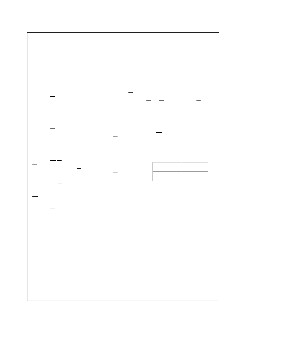
A0
This logic input is used to select one of the
ADC08062’s input multiplexer channels
A
channel is selected as shown in the table be-
low
ADC08062
Channel
A0
0
V
IN1
1
V
IN2
V
a
Positive power supply voltage input Nominal
operating supply voltage is a5V The supply
pin should be bypassed with a 10 mF bead tan-
talum in parallel with a 0 1 ceramic capacitor
Lead length should be as short as possible
http
www national com
10