Table 2. low-side mosfet losses – Rainbow Electronics MAX15034 User Manual
Page 20
MAX15034
Configurable, Single-/Dual-Output, Synchronous
Buck Controller for High-Current Applications
20
______________________________________________________________________________________
Keep the maximum output-voltage deviation less than
or equal to the adaptive voltage-positioning window
(
ΔV
OUT
). During a load step, assume a 50% contribu-
tion each from the output capacitance discharge and
the voltage drop across the ESR (
ΔV
OUT
=
ΔV
ESR_OUT
+
ΔV
Q_OUT
). Use the following equations to calculate
the required ESR and capacitance value:
where I
LOAD_STEP
is the step in load current and
t
RESPONSE
is the response time of the controller.
Controller response time depends on the control-loop
bandwidth. C
OUT
is C6 and C7 in Figure 6.
Current Limit
The MAX15034 incorporates two forward current-limit
protection mechanisms, average current limit and hic-
cup fault current limit, which accurately limit the output
current per phase. The average current-mode control
technique of the MAX15034 accurately limits the maxi-
mum average output current per phase. The
MAX15034 senses the voltage across either a sense
resistor or can implement lossless inductor sense,
sensing the voltage across the parasitic resistance of
the inductor (DCR). Use either mechanism to limit the
maximum inductor current.
The minimum average voltage, at which the voltage
across the current-sense resistor is clamped, is either
internally set to 20.4mV or is controlled by the voltage
at AVGLIMIT. The AVGLIMIT ground threshold of
550mV (typ) is the threshold above which the control of
the average current-limit voltage is transferred from the
internal 20.4mV (min) reference to the externally set
V
AVGLIMIT
. For using the internal average current-limit
value, short AVGLIMIT to AGND. The minimum (inter-
nally set) average current limit is set at:
For example, the current-sense resistor:
for a maximum output current limit of 10A. A standard
value is 2m
Ω. Also, adjust the value of the current-
sense resistor to compensate for parasitics associated
with the PCB. Select a noninductive resistor with an
appropriate wattage rating.
The implementation is shown in Figure 8.
When sensing directly across the inductor, connect an
RC circuit directly across the shunt or inductor (see
Figure 9).
R
mV
A
m
SENSE
=
=
20 4
10
2 04
.
.
Ω
I
mV
R
LIMIT MIN
SENSE
(
)
.
=
20 4
R
V
I
C
I
t
V
ESR OUT
ESR OUT
LOAD STEP
OUT
LOAD STEP
RESPONSE
Q OUT
_
_
_
_
_
=
=
×
Δ
Δ
LOSS
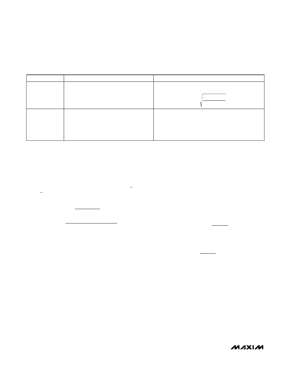
DESCRIPTION
SEGMENT LOSSES
Conduction Loss
Losses associated with MOSFET on-time, I
RMS
is a function of load current and duty cycle.
Gate Drive Loss
Losses associated with charging and
discharging the gate of the MOSFET every
cycle. There is no Q
GD
charging involved in this
MOSFET due to the zero-voltage turn-on. The
charge involved is (Q
G
- Q
GD
).
Table 2. Low-Side MOSFET Losses
P
I
R
where I
V
V
V
I
CONDUCTION
RMS
DS ON
RMS
IN
OUT
IN
LOAD
=
Ч
≈
−
Ч
2
(
)
P
V
Q
Q
f
GATEDRIVE
DD
G
GD
SW
=
Ч
(
)
Ч
−
Note: The gate drive losses are distributed between the drivers and the MOSFETs in the ratio of the gate driver’s resistance and the
MOSFET’s internal gate resistance.