Table 1. high-side mosfet losses – Rainbow Electronics MAX15034 User Manual
Page 19
MAX15034
ripple current. A low-ESR input capacitor that can han-
dle the maximum input RMS ripple current of one chan-
nel must be used. The maximum RMS capacitor ripple
current is given by:
where I
MAX
is the full load current of the regulator. V
OUT
is the output voltage of the same regulator and C
IN
is C5
in Figure 6. The ESR of the input capacitors wastes
power from the input and heats up the capacitor.
Reducing the ESR is important to maintain a high overall
efficiency and in reducing the heating of the capacitors.
Output Capacitors
The worst-case peak-to-peak inductor ripple current,
the allowable peak-to-peak output ripple voltage, and
the maximum deviation of the output voltage during
step loads determine the capacitance and the ESR
requirements for the output capacitors. The output rip-
ple can be approximated as the inductor current ripple
multiplied by the output capacitor’s ESR (R
ESR_OUT
).
The peak-to-peak inductor current ripple is given by:
During a load step, the allowable deviation of the output
voltage during the fast transient load dictates the output
capacitance and ESR. The output capacitors supply the
load step until the controller responds with a greater duty
cycle. The response time (t
RESPONSE
) depends on the
closed-loop bandwidth of the regulator. The resistive
drop across the capacitor’s ESR and capacitor discharge
causes a voltage drop during a load step. Use a combi-
nation of SP polymer and ceramic capacitors for better
transient load and ripple/noise performance.
ΔI
V
D
L f
L
OUT
SW
=
−
×
(
)
1
I
I
V
V
V
V
CIN RMS
MAX
OUT
IN
OUT
IN
(
)
(
)
≈
−
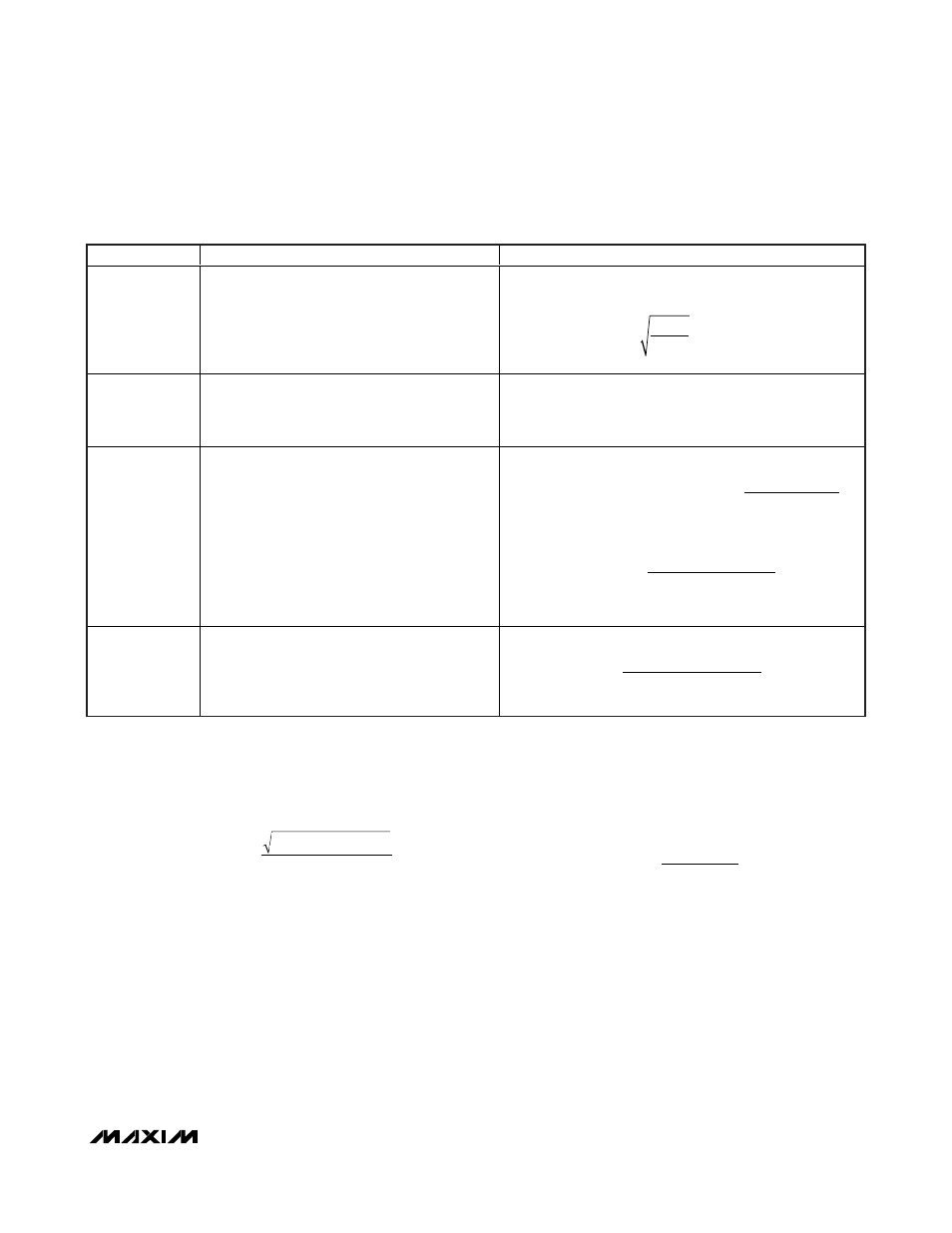
LOSS
DESCRIPTION
SEGMENT LOSS
Conduction Loss
Losses associated with MOSFET on-time and
on-resistance. I
RMS
is a function of load current
and duty cycle.
Gate Drive Loss
Losses associated with charging and
discharging the gate capacitance of the
MOSFET every cycle. Use the MOSFET’s (Q
G
)
specification.
Switching Loss
Losses during the drain voltage and drain
current transitions for every switching cycle.
Losses occur only during the Q
GS2
and Q
GD
time period and not during the initial Q
GS1
period. The initial Q
GS1
period is the rise in the
gate voltage from zero to V
TH.
R
DH_
is the high-
side MOSFET driver’s on-resistance and R
GATE
is the internal gate resistance of the high-side
MOSFET (Q
GD
and Q
GS2
are found in the
MOSFET data sheet).
Output Loss
Losses associated with Q
OSS
of the MOSFET
occur every cycle when the high-side MOSFET
turns on. The losses are caused by both
MOSFETs, but are dissipated in the high-side
MOSFET.
Table 1. High-Side MOSFET Losses
P
I
R
where I
V
V
CONDUCTION
RMS
DS ON
RMS
OUT
IN
=
Ч
≈
Ч
2
(
)
II
LOAD
P
V
Q
Q
f
GATEDRIVE
DD
G
GD
SW
=
Ч
(
)
Ч
−
P
V
I
SWITCH
IN
LOA
=
×
D
D
SW
GS
GD
GATE
f
Q
Q
I
Ч
Ч
+
(
)
2
GATE
DD
DH
where I
V
R
=
× (
_
2
++ R
GATE
)
=
+
Ч
Ч
P
Q
Q
V
f
OUTPUT
OSS HS
OSS LS
IN
SW
(
)
(
)
2
Configurable, Single-/Dual-Output, Synchronous
Buck Controller for High-Current Applications
______________________________________________________________________________________
19