Pin description – Rainbow Electronics MAX5839 User Manual
Page 7
MAX5839
Octal, 13-Bit Voltage-Output DAC
with Parallel Interface
_______________________________________________________________________________________
7
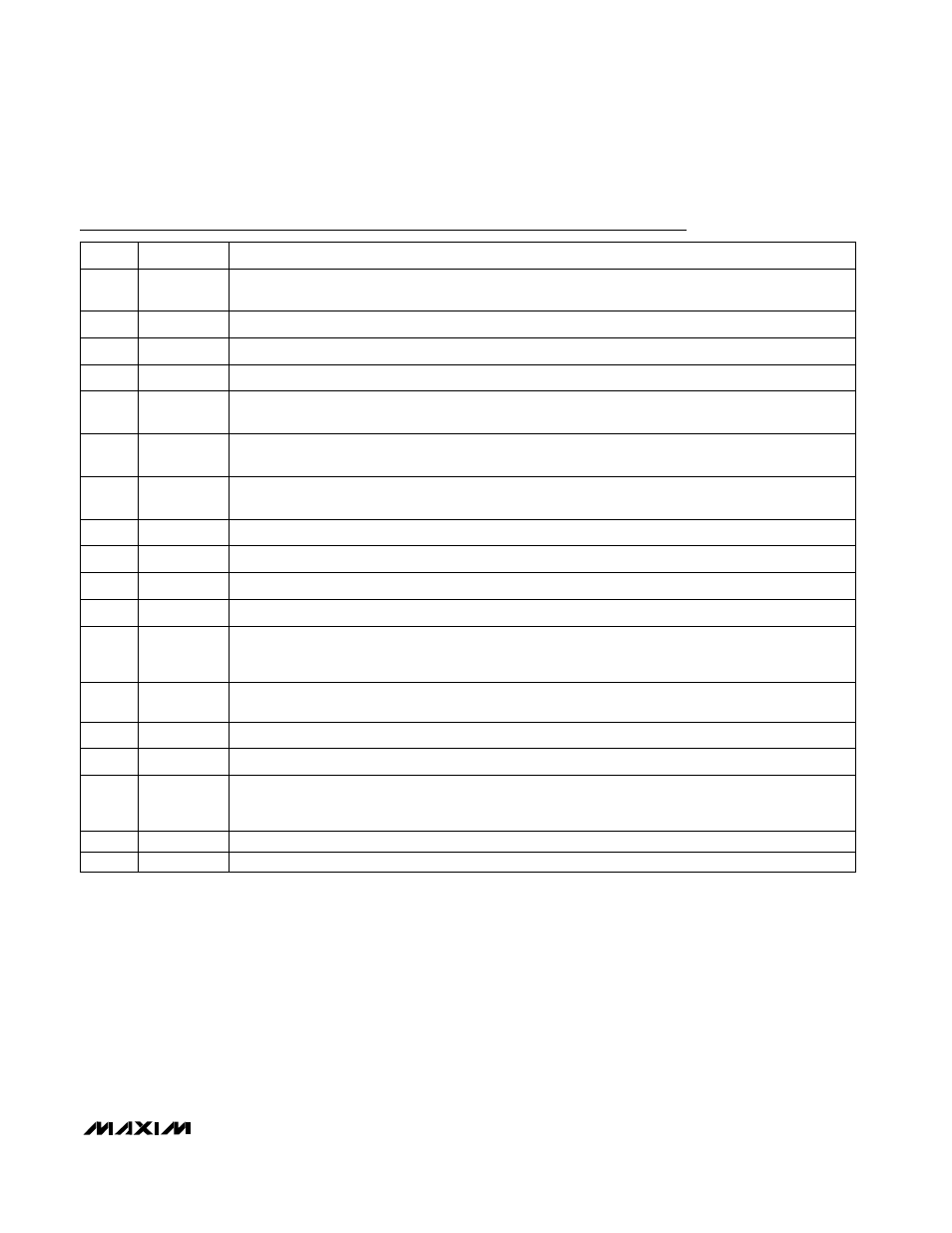
Pin Description
PIN
Device Sense Ground Input for OUTA and OUTB. In normal operation, OUTA and OUTB are referenced
to DUTGNDAB. When CLR is low, OUTA and OUTB are forced to the potential on DUTGNDAB.
DUTGNDAB
1
FUNCTION
NAME
DAC A Buffered Output Voltage
OUTA
2
Positive Reference Input for DACs A and B
REFAB+
4
Negative Reference Input for DACs A and B
REFAB-
3
Negative Analog Power Supply. Normally set to -9V. Connect both pins to the supply voltage. See
Grounding and Bypassing section for bypass requirements.
V
SS
6, 29
Address Bit 2 (MSB)
A2
8
Load Input. Drive this asynchronous input low to transfer the contents of the input latches to their
respective DAC latches. DAC latches are transparent when LD is low and latched when LD is high.
LD
7
Positive Analog Power Supply. Normally set to +14V. Connect both pins to the supply voltage. See
Grounding and Bypassing section for bypass requirements.
V
DD
5, 38
Address Bit 1
A1
9
Chip Select. Active-low input.
CS
11
Address Bit 0 (LSB)
A0
10
Write Input. Active-low strobe for conventional memory write sequence. Input data latches are transpar-
ent when WR and CS are both low. WR latches data into the DAC input latch selected by A2–A0 on the
rising edge of CS.
WR
12
Digital Power Supply. Normally set to +5V. See Grounding and Bypassing section for bypass require-
ments.
V
CC
13
Clear Input. Drive CLR low to force all DAC outputs to the voltage on their respective DUTGND _ _.
Does not affect the status of internal registers. All DACs return to their previous levels when CLR goes
high.
Data Bits 0–12. Offset binary coding.
D0–D12
15–27
Ground
GND
14
CLR
28
Positive Reference Input for DACs G and H
REFGH+
30
Negative Reference Input for DACs G and H
REFGH-
31