Table 3. analog voltage vs. digital code – Rainbow Electronics MAX5839 User Manual
Page 11
MAX5839
Octal, 13-Bit Voltage-Output DAC
with Parallel Interface
______________________________________________________________________________________
11
Table 3. Analog Voltage vs. Digital Code
The output amplifier multiplies V
DAC
by 2, yielding an
output voltage range of 2 · REF- to 2 · REF+ (Figure 1).
Further manipulation of the output voltage span is
accomplished by offsetting DUTGND. The output volt-
age of the MAX5839 is described by the following
equation:
where DATA is the numeric value of the DAC’s binary
input code, and DATA ranges from 0 (2
0
) to 8191
(2
13
- 1). The resolution of the MAX5839, defined as
1LSB, is described by the following equation:
Reference Selection
Because the MAX5839 has precision buffers on its ref-
erence inputs, the requirements for interfacing to these
inputs are minimal. Select a low-drift, low-noise refer-
ence within the recommended REF+ and REF- voltage
ranges. The MAX5839 does not require bypass capaci-
tors on its reference inputs. Add capacitors only if the
reference voltage source requires them to meet system
specifications.
Minimizing Output Glitch
The MAX5839’s internal deglitch circuitry is enabled on
the falling edge of LD. Therefore, to achieve optimum
performance, drive LD low after the inputs are either
latched or steady state. This is best accomplished by
having the falling edge of LD occur at least 50ns after
the rising edge of CS.
Power Supplies, Grounding,
and Bypassing
For optimum performance, use a multilayer PC board
with an unbroken analog ground. For normal operation,
connect the four DUTGND pins directly to the ground
plane. Avoid sharing the connections of these sensitive
pins with other ground traces.
As with any sensitive data acquisition system, connect
the digital and analog ground planes together at a sin-
gle point, preferably directly underneath the MAX5839.
Avoid routing digital signals underneath the MAX5839
to minimize their coupling into the IC.
For normal operation, bypass V
DD
and V
SS
with 0.1µF
ceramic chip capacitors to the analog ground plane. To
enhance transient response and capacitive drive capa-
bility, add 10µF tantalum capacitors in parallel with the
ceramic capacitors. Note, however, that the MAX5839
does not require the additional capacitance for stability.
Bypass V
CC
with a 0.1µF ceramic chip capacitor to the
digital ground plane.
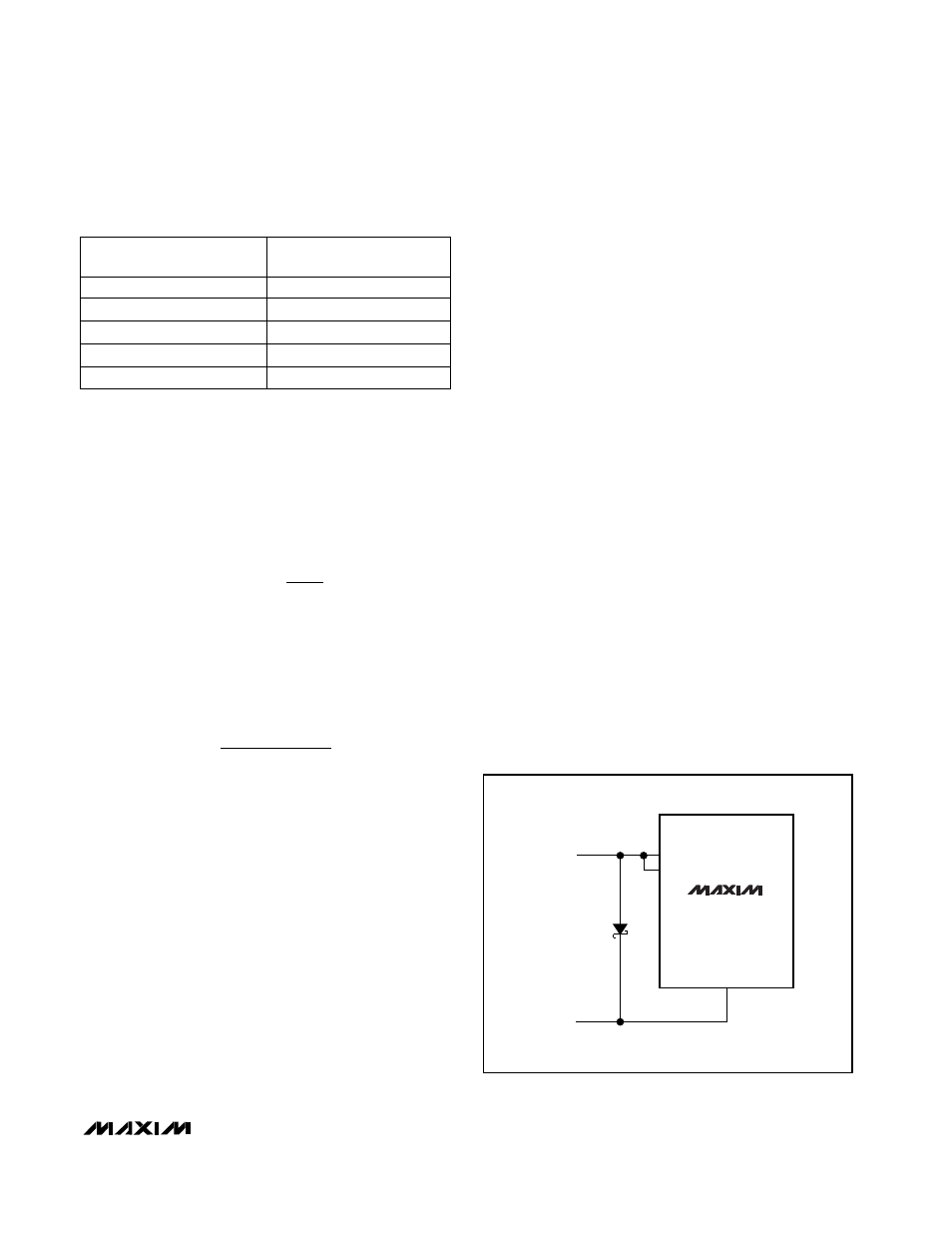
Power-Supply Sequencing
To guarantee proper operation of the MAX5839, ensure
that power is applied to V
DD
before V
SS
and V
CC
. Also
ensure that V
SS
is never more than 300mV above
ground. To prevent this situation, connect a Schottky
diode between V
SS
and the analog ground plane, as
shown in Figure 3. Do not power up the logic input pins
before establishing the supply voltages. If this is not
possible and the digital lines can drive more than
10mA, place current-limiting resistors (e.g., 470
Ω) in
series with the logic pins.
LSB
2 REF REF
2
13
=
+ −
−
(
)
V
2 V
V
DATA
2
V
V
OUT
REF
REF
13
REF
OUTGND
=
−
(
)
+
−
+
−
−
INPUT CODE
0 0000 0000 0001
1 1111 1111 1111
0 1001 1101 1001
1 0000 0000 0000
0 0000 0000 0000
OUTPUT
VOLTAGE (V)
-3.998586
+8.998413
+600µ
+4.500
-4.000
Note: Output voltage is based on REF+ = +4.5V, REF- = -2.0V,
and DUTGND = 0.
GND
V
SS
SYSTEM GND
1N5817
MAX5839
V
SS
V
SS
Figure 3. Schottky Diode Between V
SS
and GND