Applications information – Rainbow Electronics MAX5839 User Manual
Page 10
MAX5839
Octal, 13-Bit Voltage-Output DAC
with Parallel Interface
10
______________________________________________________________________________________
Digital Inputs and Interface Logic
All digital inputs are compatible with both TTL and
CMOS logic. The MAX5839 interfaces with micro-
processors using a data bus at least 13 bits wide. The
interface is double buffered, allowing simultaneous
updating of all DACs. There are two latches for each
DAC (see Functional Diagram): an input latch that
receives data from the data bus, and a DAC latch that
receives data from the input latch. Address lines A0,
A1, and A2 select which DAC’s input latch receives
data from the data bus, as shown in Table 1. Both the
input latches and the DAC latches are transparent
when CS, WR, and LD are all low. Any change of
D0–D12 during this condition appears at the output
instantly. Transfer data from the input latches to the
DAC latches by asserting the asynchronous LD signal.
Each DAC’s analog output reflects the data held in its
DAC latch. All control inputs are level triggered. Table 2
is an interface truth table.
Input Write Cycle
Data can be latched or transferred directly to the DAC.
CS and WR control the input latch, and LD transfers
information from the input latch to the DAC latch. The
input latch is transparent when CS and WR are low,
and the DAC latch is transparent when LD is low. The
address lines (A0, A1, A2) must be valid for the dura-
tion that CS and WR are low (Figure 1), to prevent data
from being inadvertently written to the wrong DAC.
Data is latched within the input latch when either CS or
WR is high.
Loading the DACs
Taking LD high latches data into the DAC latches. If LD
is brought low when WR and CS are low, the DAC
addressed by A0, A1, and A2 is directly controlled by
the data on D0–D12. This allows the maximum digital
update rate; however, it is sensitive to any glitches or
skew in the input data stream.
Asynchronous Clear
The MAX5839 has an asynchronous clear pin (CLR)
that, when asserted, sets all DAC outputs to the voltage
present on their respective DUTGND pins. Deassert
CLR to return the DAC output to its previous voltage.
Note that CLR does not clear any of the internal digital
registers.
Applications Information
Multiplying Operation
The MAX5839 can be used for multiplying applications.
Its reference accepts both DC and AC signals. Since
the reference inputs are unipolar, multiplying operation
is limited to two quadrants. See the graphs in the
Typical Operating Characteristics for dynamic perfor-
mance of the DACs and output buffers.
Digital Code and
Analog Output Voltage
The MAX5839 uses offset binary coding. A 13-bit two’s
complement code is converted to a 13-bit offset binary
code by adding 2
12
= 4096.
Output Voltage Range
For typical operation, connect DUTGND to signal
ground, V
REF
+ to +4.5V, and V
REF
- to -2.0V. Table 3
shows the relationship between digital code and output
voltage.
The DAC digital code controls each leg of the 13-bit
R-2R ladder. A code of 0x0 connects all legs of the lad-
der to REF-, corresponding to a DAC output voltage
(V
DAC
) equal to REF-. A code of 0x1FFF connects all
legs of the ladder to REF+, corresponding to a V
DAC
approximately equal to REF+.
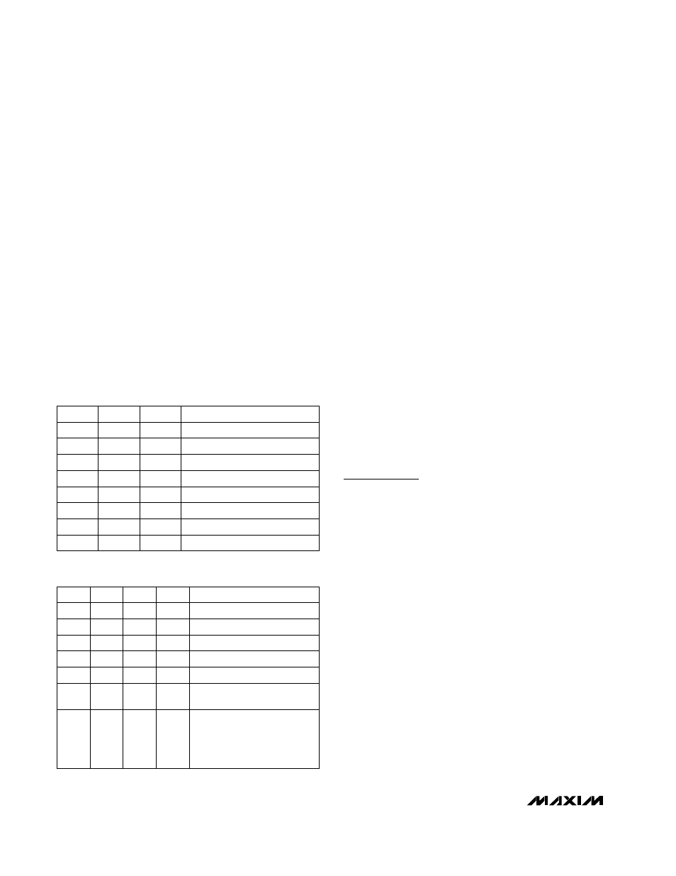
A2
FUNCTION
DAC A input latch
0
DAC C input latch
0
DAC B input latch
0
DAC D input latch
0
DAC H input latch
1
DAC E input latch
1
DAC G input latch
1
DAC F input latch
1
A1
1
0
1
1
0
0
1
0
A0
1
0
0
1
1
0
0
1
CLR
DAC register transparent
FUNCTION
X
Input register transparent
X
Input register latched
X
Input register latched
X
DAC register latched
X
Outputs of DACs set to volt-
age defined by the DAC
register, the references,
and the corresponding
DUTGND_ _
1
Outputs of DACs at
DUTGND_ _
0
LD
0
X
X
X
1
1
X
WR
X
0
1
X
X
X
X
Table 1. MAX5839 DAC Addressing
Table 2. Interface Truth Table
CS
X
0
X
1
X
X
X
X = Don’t care