Rainbow Electronics MAX8805Z User Manual
Page 2

MAX8805Y/MAX8805Z
600mA PWM Step-Down Converters in
2mm x 2mm WLP for WCDMA PA Power
2
_______________________________________________________________________________________
ABSOLUTE MAXIMUM RATINGS
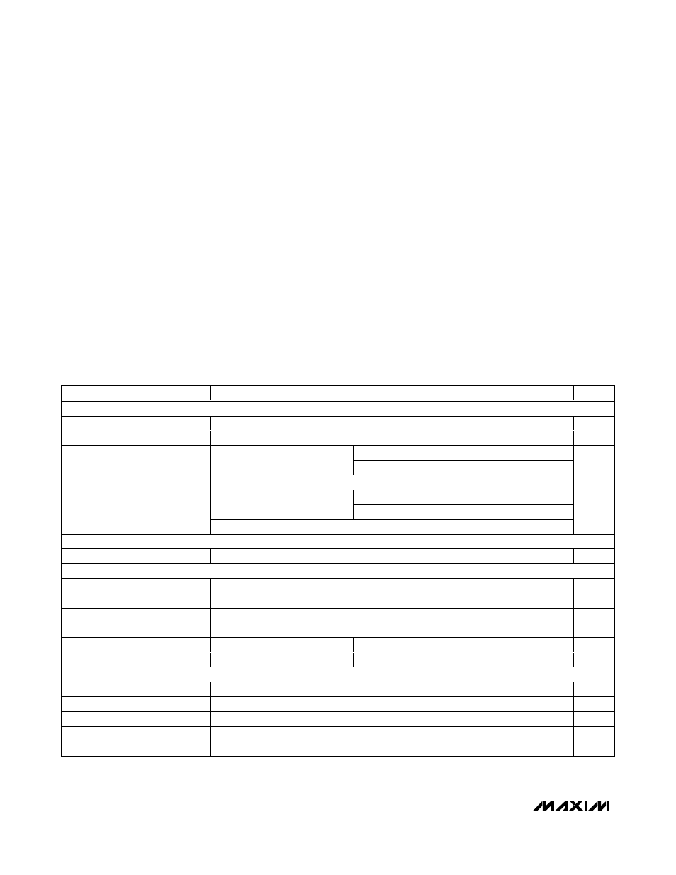
ELECTRICAL CHARACTERISTICS
(V
IN1A
= V
IN1B
= V
IN2
= V
PA_EN
= V
EN1
= V
EN2
= 3.6V, V
HP
= 0V, V
REFIN
= 0.9V, T
A
= -40°C to +85°C. Typical values are at T
A
=
+25°C, unless otherwise noted.) (Note 1)
Stresses beyond those listed under “Absolute Maximum Ratings” may cause permanent damage to the device. These are stress ratings only, and functional
operation of the device at these or any other conditions beyond those indicated in the operational sections of the specifications is not implied. Exposure to
absolute maximum rating conditions for extended periods may affect device reliability.
IN1A, IN1B, IN2, REFIN, EN2, REFBP to AGND ...-0.3V to +6.0V
PAA, PAB, PA_EN, HP to AGND....-0.3V to (V
IN1A
/V
IN1B
+ 0.3V)
LDO1, LDO2, EN1 to AGND ......................-0.3V to (V
IN2
+ 0.3V)
IN2 to IN1B/IN1A ...................................................-0.3V to +0.3V
PGND to AGND .....................................................-0.3V to +0.3V
LX Current ......................................................................0.7A
RMS
IN1A/IN1B and PAA/PAB Current .....................................2A
RMS
PAA and PAB Short Circuit to GND or IN...................Continuous
Continuous Power Dissipation (T
A
= +70°C)
16-Bump WLP (derate 12.5mW/°C above +70°C).............1W
Junction Temperature ......................................................+150°C
Storage Temperature Range .............................-65°C to +150°C
Bump Temperature (soldering, reflow) ............................+235°C
PARAMETER
CONDITIONS
MIN
TYP
MAX
UNITS
INPUT SUPPLY
Input Voltage
V
IN1A
, V
IN1B
, V
IN2
2.7
5.5
V
Input Undervoltage Threshold
V
IN1A
, V
IN1B
, V
IN2
rising, 180mV typical hysteresis
2.52
2.63
2.70
V
T
A
= +25°C
0.1
4
Shutdown Supply Current
V
PA_EN
= V
EN1
= V
EN2
= 0V
T
A
= +85°C
0.1
µA
V
PA_EN
= 0V, I
LDO1
= I
LDO2
= 0A
150
250
MAX8805Y
3500
V
EN1
= V
EN2
= 0V, I
PA
= 0A,
switching
MAX8805Z
5000
No-Load Supply Current
V
EN1
= V
EN2
= 0V, V
HP
= 3.6V
150
µA
THERMAL PROTECTION
Thermal Shutdown
T
A
rising, 20°C typical hysteresis
+160
°C
LOGIC CONTROL
PA_EN, EN1, EN2, HP Logic-
Input High Voltage
2.7V
≤ V
IN1A
= V
IN1B
= V
IN2
≤ 5.5V
1.4
V
PA_EN, EN1, EN2, HP Logic-
Input Low Voltage
2.7V
≤ V
IN1A
= V
IN1B
= V
IN2
≤ 5.5V
0.4
V
T
A
= +25°C
0.01
1
Logic-Input Current
(PA_EN, EN1, EN2, HP)
V
IL
= 0V or V
IH
= V
IN1A
= 5.5V
T
A
= +85°C
0.1
µA
REFIN
REFIN Common-Mode Range
0.1
2.2
V
REFIN to PA_ Gain (Falling Edge)
V
REFIN
= 0.4V, 0.9V, 1.7V, 2.2V
1.96
2.00
2.04
V/V
REFIN Input Resistance
540
k
Ω
REFIN
Dual Mode™ Threshold
V
REFIN
rising, 50mV hysteresis
0.45 x
V
IN2
0.465 x
V
IN2
0.48 x
V
IN2
V
Note: This device is constructed using a unique set of packaging techniques that impose a limit on the thermal profile the device
can be exposed to during board level solder attach and rework. This limit permits only the use of the solder profiles recom-
mended in the industry-standard specification, JEDEC 020A, paragraph 7.6, Table 3 for IR/VPR and Convection reflow.
Preheating is required. Hand or wave soldering is not allowed.
Dual Mode is a trademark of Maxim Integrated Products, Inc.
