Detailed description – Rainbow Electronics MAX8805Z User Manual
Page 13

MAX8805Y/MAX8805Z
600mA PWM Step-Down Converters in
2mm x 2mm WLP for WCDMA PA Power
______________________________________________________________________________________
13
Detailed Description
The MAX8805Y/MAX8805Z are designed to dynamical-
ly power the PA in WCDMA and NCDMA handsets. The
devices contain a high-frequency, high-efficiency step-
down converter, and two LDOs. The step-down convert-
er delivers over 600mA. The hysteretic PWM control
scheme provides extremely fast transient response,
while 2MHz and 4MHz switching-frequency options
allow the trade-off between efficiency and the smallest
external components. A 60m
Ω bypass FET connects
the PA directly to the battery during high-power trans-
mission.
Step-Down Converter Control Scheme
A hysteretic PWM control scheme ensures high effi-
ciency, fast switching, fast transient response, low-out-
put ripple, and physically tiny external components.
The control scheme is simple: when the output voltage
is below the regulation threshold, the error comparator
begins a switching cycle by turning on the high-side
switch. This high-side switch remains on until the mini-
mum on-time expires and the output voltage is within
regulation, or the inductor current is above the current-
limit threshold. Once off, the high-side switch remains
off until the minimum off-time expires and the output
voltage falls again below the regulation threshold.
During the off period, the low-side synchronous rectifier
turns on and remains on until the high-side switch turns
on again. The internal synchronous rectifier eliminates
the need for an external Schottky diode.
Voltage-Positioning Load Regulation
The MAX8805Y/MAX8805Z step-down converters utilize
a unique feedback network. By taking DC feedback
from the LX node through R1 in Figure 1, the usual
phase lag due to the output capacitor is removed, mak-
ing the loop exceedingly stable and allowing the use of
very small ceramic output capacitors. To improve the
load regulation, resistor R3 is included in the feedback.
This configuration yields load regulation equal to half of
the inductor’s series resistance multiplied by the load
current. This voltage-positioning load regulation greatly
reduces overshoot during load transients or when
changing the output voltage from one level to another.
However, when calculating the required REFIN voltage,
the load regulation should be considered. Because
inductor resistance is typically well specified and the
typical PA is a resistive load, the MAX8805Y/MAX8805Z
V
REFIN
to V
OUT
gain is slightly less than 2V/V.
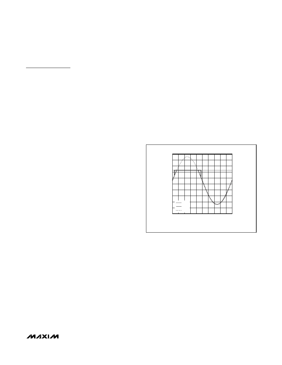
Step-Down Converter Bypass Mode
During high-power transmission, the bypass mode con-
nects IN1A and IN1B directly to PAA and PAB with the
internal 60m
Ω (typ) bypass FET, while the step-down
converter is forced into 100% duty-cycle operation. The
low on-resistance in this mode provides low dropout,
long battery life, and high output current capability.
Forced and Automatic Bypass Mode
Invoke forced bypass mode by driving HP high or
invoke automatic bypass mode by applying a high volt-
age to REFIN. To prevent excessive output ripple as the
step-down converter approaches dropout, the
MAX8805Y/MAX8805Z enter bypass mode automatically
when V
REFIN
> 0.465 x V
IN2
(see Figure 2). Note that
IN2 is used instead of IN1 to prevent switching noise
from causing false enagement of automatic bypass
mode. For this reason, IN2 must be connected to the
same source as IN1.
Shutdown Mode
Connect PA_EN to GND or logic-low to place the
MAX8805Y/MAX8805Z PA step-down converter in shut-
down mode. In shutdown, the control circuitry, internal
switching MOSFET, and synchronous rectifier turn off
and LX becomes high impedance. Connect PA_EN to
IN1_ or logic-high for normal operation.
Connect EN1 or EN2 to GND or logic-low to place
LDO1 or LDO2, respectively, in shutdown mode. In
shutdown, the outputs of the LDOs are pulled to ground
through an internal 1k
Ω resistor.
When the PA step-down and LDOs are all in shutdown,
the MAX8805Y/MAX8805Z enter a very low power
state, where the input current drops to 0.1µA (typ).
0
1.0
0.5
2.0
1.5
3.0
2.5
3.5
4.5
4.0
5.0
0
10 15 20
5
25 30 35
45
40
50
TIME (ms)
IN2 AND PA_
VOLTAGE (V)
REFIN VOLTAGE (V)
IN2
PA_
REFIN
0
0.5
1.0
1.5
2.0
2.5
Figure 2. V
IN2
and V
PA_
with Automatic Entry/Exit into Bypass
Mode
