Electrical characteristics (continued) – Rainbow Electronics MAX5547 User Manual
Page 3
MAX5547
Dual, 10-Bit, Current-Sink Output DAC
_______________________________________________________________________________________
3
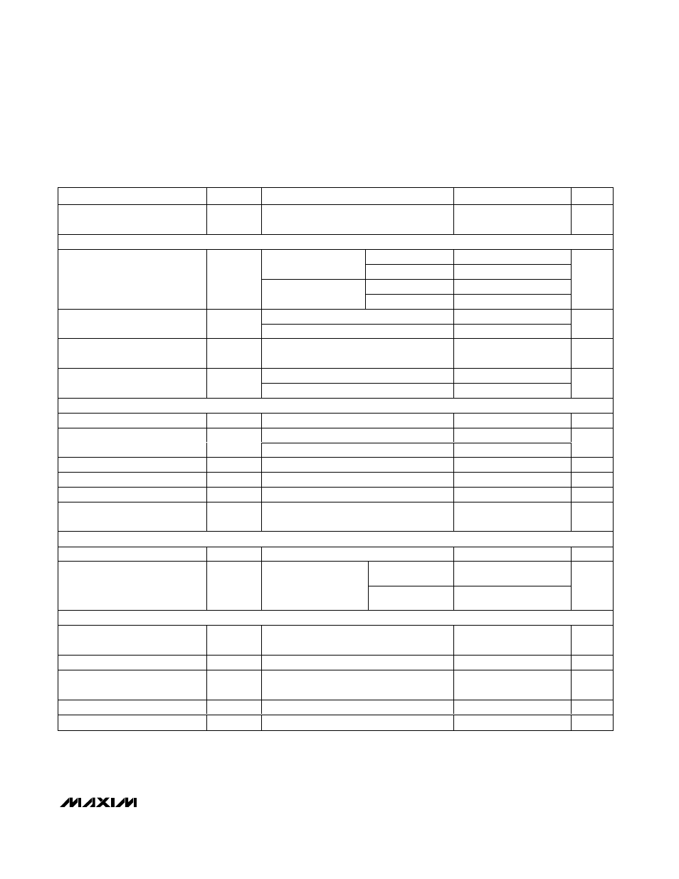
ELECTRICAL CHARACTERISTICS (continued)
(V
DD
= +2.7 to +5.25V, GND = 0, external reference = +2.5V, output voltage = +2.0V, T
A
= -40°C to +85°C. Typical values are at
V
DD
= +3.0V, and T
A
= +25°C.) (Note 1)
PARAMETER
SYMBOL
CONDITIONS
MIN
TYP
MAX
UNITS
External-Reference Input
Impedance
R
REF
90
k
Ω
DAC OUTPUTS
Code = 030h
50
1.2mA low-current
range
Code = 3FFh
1170
1200
1230
Code = 030h
150
Output Current (Note 4)
I
OUT
_
3.6mA high-current
range
Code = 3FFh
3400
3600
3800
µA
1.2mA full-scale current
1.17
LSB Size
3.6mA full-scale current
3.52
µA
Current-Source Compliance
Voltage Range
I
OUT
_ = full-scale (Note 5)
0.8
V
DD
V
I
OUT
_ = 1.2mA
800
Output Impedance at Full-Scale
Current
I
OUT
_ = 3.6mA
180
k
Ω
DYNAMIC PERFORMANCE
Settling Time
t
S
To 1% (Note 6)
10
µs
f = 0.1Hz to 10Hz
0.05
Output Noise
I
RMS
f = 10Hz to 10kHz
0.35
LSB
RMS
Supply Feedthrough
100mV, 1kHz signal added to V
DD
0.85
LSB/V
Digital Feedthrough
R
LOAD
= 500
Ω, C
LOAD
= 100pF
2
pA
·
s
Digital-to-Analog Glitch Impulse
R
LOAD
= 500
Ω, C
LOAD
= 100pF
16
pA
·
s
DAC-to-DAC Full-Scale Current
Matching
2
%
POWER SUPPLIES
Supply Voltage
V
DD
+2.70
+5.25
V
Internal reference
mode
1.1
2
Supply Current
I
DD
V
DD
= +5.25V, no load,
SCLK not switching
External reference
mode
0.75
1.5
mA
LOGIC AND CONTROL INPUTS
Input High Voltage
V
IH
(Note 7)
0.7 x
V
DD
V
Input Low Voltage
V
IL
(Note 7)
0.8
V
Input Hysteresis
V
HYS
0.05 x
V
DD
V
Input Capacitance
C
IN
10
pF
Input Leakage Current
I
IN
±1
µA