Max4880, Applications information – Rainbow Electronics MAX4880 User Manual
Page 8

MAX4880
and turns back on when the battery falls below the BTB
trip level minus BTB hysteresis. Drive CB low to turn off
the internal switch, regardless of the battery voltage.
This control bit can be used to provide additional top-
off charge for the battery. When the CB pin is cycled,
the internal battery switch is turned on and off. This
effectively provides an average current that is lower
than the full-charge current.
GATE Driver
An on-chip charge pump drives the GATE voltage to
approximately twice V
IN
, allowing the use of a low-cost,
n-channel MOSFET (
Figure
5). The actual GATE output
voltage tracks approximately 2 x V
IN,
until V
IN
exceeds
the OVLO trip level, 5.6V (typ). The GATE output volt-
age, as a function of input voltage, is shown in the
Typical Operating Characteristics.
Applications Information
MOSFET Selection
The MAX4880 is designed for use with an n-channel
MOSFET. MOSFETs with R
DS(ON)
specified for a V
GS
of
4.5V are ideal. If the input supply is near the UVLO min-
imum of 4.2V, consider using a MOSFET specified for a
lower V
GS
voltage. Also, the V
DS
should be 30V for the
MOSFET to withstand the full 28V IN range of the
MAX4880.
Table
1 shows a selection of MOSFETs
appropriate for use with the MAX4880.
IN Bypass Considerations
Bypass IN to GND with a 1µF ceramic capacitor to
achieve 15kV ESD-protected input. When the power
source has significant inductance due to long lead
length, take care to prevent overshoots due to the LC
Overvoltage-Protection Controller with
Internal Disconnect Switch
8
_______________________________________________________________________________________
CHARGE-CURRENT-
LIMIT RESISTOR
DISCHARGE
RESISTANCE
STORAGE
CAPACITOR
Cs
150pF
R
C
50
Ω to 100Ω
R
D
330
Ω
HIGH-
VOLTAGE
DC
SOURCE
DEVICE
UNDER
TEST
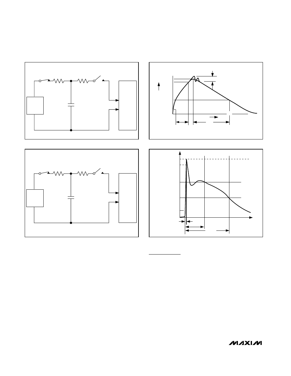
Figure 8. IEC 61000-4-2 ESD Test Model
CHARGE-CURRENT-
LIMIT RESISTOR
DISCHARGE
RESISTANCE
STORAGE
CAPACITOR
Cs
100pF
R
C
1M
Ω
R
D
1.5k
Ω
HIGH-
VOLTAGE
DC
SOURCE
DEVICE
UNDER
TEST
Figure 6. Human-Body ESD Test Model
I
P
100%
90%
36.8%
t
RL
TIME
t
DL
CURRENT WAVEFORM
PEAK-TO-PEAK RINGING
(NOT DRAWN TO SCALE)
Ir
10%
0
0
AMPERES
Figure 7. Human-Body-Model Current Waveform
tr = 0.7ns TO 1ns
30ns
60ns
t
100%
90%
10%
I
PEAK
I
Figure
9. IEC 61000-4-2 ESD Generator Current
