Max9712 – Rainbow Electronics MAX9712 User Manual
Page 2
500mW, Low EMI, Filterless,
Class D Audio Amplifier
2
_______________________________________________________________________________________
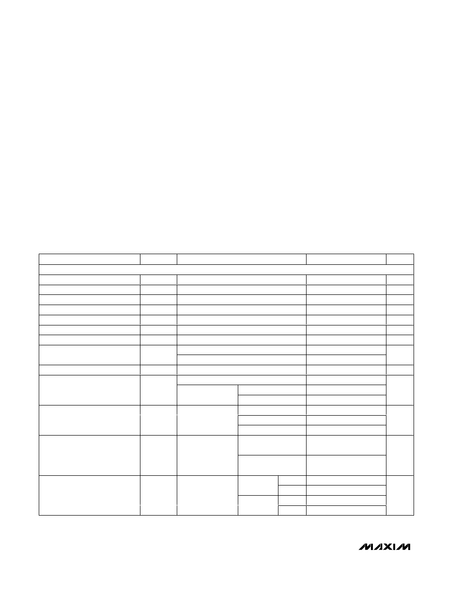
ABSOLUTE MAXIMUM RATINGS
ELECTRICAL CHARACTERISTICS
(V
DD
= PV
DD
= SHDN = 3.3V, GND = PGND = 0V, SYNC = GND (FFM), R
L
= 8
Ω, R
L
connected between OUT+ and OUT-, T
A
=
T
MIN
to T
MAX
, unless otherwise noted. Typical values are at T
A
= +25°C.) (Notes 1, 2)
Stresses beyond those listed under “Absolute Maximum Ratings” may cause permanent damage to the device. These are stress ratings only, and functional
operation of the device at these or any other conditions beyond those indicated in the operational sections of the specifications is not implied. Exposure to
absolute maximum rating conditions for extended periods may affect device reliability.
V
DD
to GND..............................................................................6V
PV
DD
to PGND .........................................................................6V
GND to PGND .......................................................-0.3V to +0.3V
All Other Pins to GND.................................-0.3V to (V
DD
+ 0.3V)
Continuous Current Into/Out of PV
DD
/PGND/OUT_ ........
±600mA
Continuous Input Current (all other pins)..........................
±20mA
Duration of OUT_ Short Circuit to GND or PV
DD
........Continuous
Duration of Short Circuit Between OUT+ and OUT- ..Continuous
Continuous Power Dissipation (T
A
= +70°C)
10-Pin TDFN (derate 24.4mW/°C above +70°C) .....1951.2mW
10-Pin µMAX (derate 5.6mW/
o
C above +70°C) .........444.4mW
12-Bump UCSP (derate 6.1mW/°C above +70°C)........484mW
Junction Temperature ......................................................+150°C
Operating Temperature Range ...........................-40°C to +85°C
Storage Temperature Range .............................-65°C to +150°C
Lead Temperature (soldering, 10s) .................................+300°C
Bump Temperature (soldering)
Reflow ..........................................................................+235°C
MAX9712
PARAMETER
SYMBOL
CONDITIONS
MIN
TYP
MAX
UNITS
GENERAL
Supply Voltage Range
V
DD
Inferred from PSRR test
2.5
5.5
V
Quiescent Current
I
DD
4
5.2
mA
Shutdown Current
I
SHDN
0.1
5
µA
Turn-On Time
t
ON
30
ms
Input Resistance
R
IN
T
A
= +25°C
14
20
k
Ω
Input Bias Voltage
V
BIAS
Either input
0.73
0.83
0.93
V
Voltage Gain
A
V
3.8
4
4.2
V/V
T
A
= +25°C
±11
40
Output Offset Voltage
V
OS
T
MIN
≤ T
A
≤ T
MAX
±65
mV
Common-Mode Rejection Ratio
CMRR
f
IN
= 1kHz, input referred
72
dB
V
DD
= 2.5V to 5.5V
50
70
f
RIPPLE
= 217Hz
72
Power-Supply Rejection Ratio
(Note 3)
PSRR
200mV
P-P
ripple
f
RIPPLE
= 20kHz
55
dB
R
L
= 16
Ω, V
DD
= 5V
700
R
L
= 8
Ω
450
Output Power
P
OUT
THD+N = 1%
R
L
= 6
Ω
250
mW
R
L
= 8
Ω,
P
OUT
= 125mW
0.01
Total Harmonic Distortion Plus
Noise
THD+N
f
IN
= 1kHz, either
FFM or SSM
R
L
= 6
Ω,
P
OUT
= 125mW
0.01
%
FFM
88
BW = 22Hz
to 22kHz
SSM
86
FFM
91
Signal-to-Noise Ratio
SNR
V
OUT
= 1.8V
RMS
A-weighted
SSM
89
dB