Electrical characteristics, Absolute maximum ratings – Rainbow Electronics MAX14541Е User Manual
Page 2
3-Channel, Low-Leakage ESD Protector
MAX14541E
2 ______________________________________________________________________________________
Stresses beyond those listed under “Absolute Maximum Ratings” may cause permanent damage to the device. These are stress ratings only, and functional operation of the device at these
or any other conditions beyond those indicated in the operational sections of the specifications is not implied. Exposure to absolute maximum rating conditions for extended periods may
affect device reliability.
(Voltages referenced to GND.)
V
CC
to GND ...........................................................-0.3V to +18V
I/O-1, I/O-2, I/O-3 to GND ........................ -0.3V to (V
CC
+ 0.3V)
Continuous Power Dissipation (T
A
= +70NC)
5-Pin SC70 (derate 3.1mW/NC above +70NC) .........246.9mW
Thermal Resistance (Note 1)
B
JA
.............................................................................324NC/W
B
JC
............................................................................115NC/W
Operating Temperature Range ........................ -40NC to +125NC
Storage Temperature Range ............................ -65NC to +150NC
Junction Temperature .....................................................+150NC
Lead Temperature (soldering, 10s) ................................+300NC
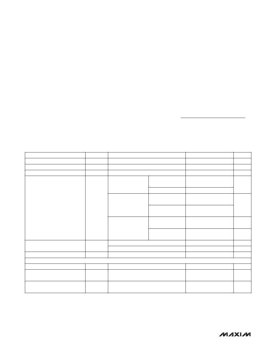
ELECTRICAL CHARACTERISTICS
(V
CC
= +5V, T
A
= T
MIN
to T
MAX
, unless otherwise noted. Typical values are at T
A
= +25NC.) (Note 2)
ABSOLUTE MAXIMUM RATINGS
Note 1: Package thermal resistances were obtained using the method described in JEDEC specification JESD51-7, using a four-
layer board. For detailed information on package thermal considerations, refer to
.
Note 2: Parameters are 100% production tested at TA = +25°C. Specifications over temperature guaranteed by design only.
Note 3: Idealized clamp voltages. See the Applications Information section for more information.
Note 4: Guaranteed by design, not production tested.
PARAMETER
SYMBOL
CONDITIONS
MIN
TYP
MAX
UNITS
Supply Voltage
V
CC
0.9
16
V
Supply Current
I
CC
1
100
nA
Diode Forward Voltage
V
F
I
F
= 10mA, T
A
= +25°C
0.65
0.95
V
Channel Clamp Voltage
(Note 3)
V
C
T
A
= +25°C, ±15kV
Human Body Model,
I
F
= 10A
Positive transients
V
CC
+
25
V
Negative transients
-25
T
A
= +25°C, ±8kV
Contact Discharge
(IEC 61000-4-2),
I
F
= 24A
Positive transients
V
CC
+
60
V
Negative transients
-60
T
A
= +25°C, ±15kV
Air-Gap Discharge
(IEC 61000-4-2),
I
F
= 45A
Positive transients
V
CC
+
100
V
Negative transients
-100
V
Channel Leakage Current
(Note 4)
T
A
= -40°C to +50°C
-1
+1
nA
T
A
= -40°C to +125°C
-1
+1
µA
I/O Capacitance
Bias of V
CC
/2, f = 1MHz (Note 4)
6
7
pF
ESD PROTECTION
Human Body Model
±15
kV
IEC 61000-4-2 Air-Gap
Discharge
±15
kV
IEC 61000-4-2 Contact
Discharge
±8
kV