Rainbow Electronics MAX5157 User Manual
Page 11
The MAX5156/MAX5157’s digital inputs are double
buffered, which allows any of the following: loading the
input register(s) without updating the DAC register(s),
updating the DAC register(s) from the input register(s),
or updating the input and DAC registers concurrently.
The address and control bits allow the DACs to act
independently.
Send the 16-bit data as one 16-bit word (QSPI) or two
8-bit packets (SPI, Microwire), with CS low during this
period. The address and control bits determine which
register will be updated, and the state of the registers
when exiting shutdown. The 3-bit address/control
determines the following:
•
registers to be updated
•
clock edge on which data is clocked out via the seri-
al data output (DOUT)
•
state of the user-programmable logic output
•
configuration of the device after shutdown
The general timing diagram in Figure 5 illustrates how
data is acquired. Driving CS low enables the device to
receive data. Otherwise, the interface control circuitry is
disabled. With CS low, data at DIN is clocked into the
register on the rising edge of SCLK. As CS goes high,
data is latched into the input and/or DAC registers
depending on the address and control bits. The maxi-
mum clock frequency guaranteed for proper operation
is 10MHz. Figure 6 depicts a more detailed timing dia-
gram of the serial interface.
Serial Data Output (DOUT)
DOUT is the internal shift register’s output. It allows for
daisy-chaining and data readback. The MAX5156/
MAX5157 can be programmed to shift data out of
DOUT on SCLK’s falling edge (Mode 0) or rising edge
(Mode 1). Mode 0 provides a lag of 16 clock cycles,
which maintains compatibility with SPI/QSPI and
Microwire interfaces. In Mode 1, the output data lags
15.5 clock cycles. On power-up, the device defaults to
Mode 0.
User-Programmable Logic Output (UPO)
UPO allows an external device to be controlled through
the MAX5156/MAX5157 serial interface (Table 1), there-
by reducing the number of microcontroller I/O pins
required. On power-up, UPO is low.
Power-Down Lockout Input (
PDL
)
PDL disables software shutdown when low. When in
shutdown, transitioning PDL from high to low wakes up
the part with the output set to the state prior to shut-
down. PDL can also be used to asynchronously wake
up the device.
MAX5156/MAX5157
Low-Power, Dual, 12-Bit Voltage-Output DACs
with Configurable Outputs
______________________________________________________________________________________
11
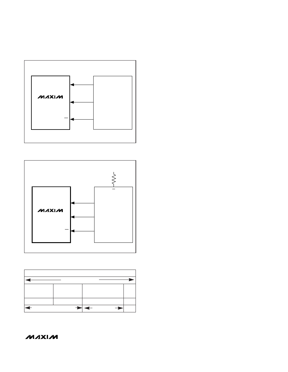
SCLK
DIN
CS
SK
SO
I/O
MAX5156
MAX5157
MICROWIRE
PORT
Figure 2. Connections for Microwire
DIN
SCLK
CS
MOSI
SCK
I/O
SPI/QSPI
PORT
SS
V
CC
CPOL = 0, CPHA = 0
MAX5156
MAX5157
Figure 3. Connections for SPI/QSPI
Figure 4. Serial-Data Format
1 Address/2 Control Bits
A0
0
Address Bits
C1, C0
Control Bits
S0
12 Data Bits
D11.......................D0
MSB...DataBits...LSB
Sub
Bit
16 Bits of Serial Data
MSB...................................................................................LSB