Rainbow Electronics MAX15001 User Manual
Page 15
Layout Recommendations
Typically, there are two sources of noise emission in a
switching power supply: high di/dt loops and high dv/dt
surfaces. For example, traces that carry the drain cur-
rent often form high di/dt loops. Similarly, the heatsink
of the MOSFET presents a dv/dt source; therefore, mini-
mize the surface area of the heatsink as much as possi-
ble. Keep all PC board traces carrying switching
currents as short as possible to minimize current loops.
Use a ground plane for best results. The pins of the
µMAX package are positioned to allow easy interfacing
to the external MOSFET.
For universal AC input design, follow all applicable
safety regulations. Offline power supplies may require
UL, VDE, and other similar agency approvals. To avoid
noise coupling of signals from RT to NDRV, route traces
from RT away from NDRV.
MAX15000/MAX15001
Current-Mode PWM Controllers with
Programmable Switching Frequency
______________________________________________________________________________________
15
V
CC
COMP
FB
GND
CS
NDRV
UVLO/EN
0V
12V
R2
R3
R1
C1
RT
UFLG
C6
R15
R12
C4
IN
MAX15001
C2
C3
R5
R6
15V
D1
Q1
L1
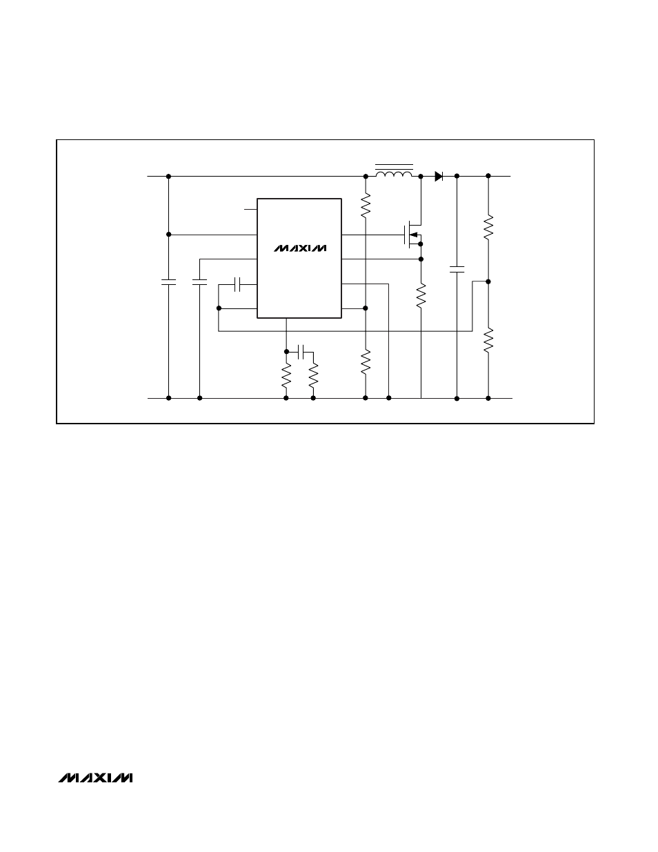
Figure 8. 12V to 15V Output Boost Regulator