Rainbow Electronics MAX15001 User Manual
Page 14

MAX15000/MAX15001
Primary-Side-Regulated,
Isolated Telecom Power Supply
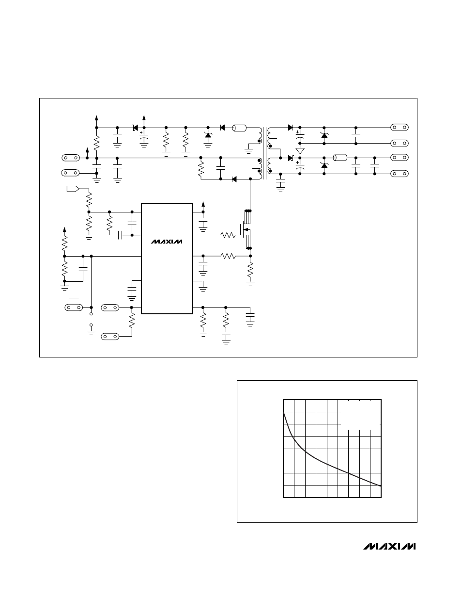
Figure 6 shows a complete circuit of a dual-output
power supply with a telecom voltage range of 36V to
72V. An important aspect of this power supply is that it
is primary-side regulated. The regulation through the
tertiary winding also supplies bias for the MAX15000.
In the circuit of Figure 6, cross-regulation has been
improved (tertiary and 5V outputs) by using chip induc-
tors, L1 and L2, and R7||R12 across C12. R7||R12 pre-
sents enough loading on the tertiary winding output to
allow ±10% load regulation on the 5V output over a
load current range from 150mA to 1.5A (Figure 7).
Current-Mode PWM Controllers with
Programmable Switching Frequency
14
______________________________________________________________________________________
MAX15000A
U1
+VIN
UFLG
-VIN
VOUT2
15V/100mA
5V/1.5A
SGND
VOUT1
SGND
1
2
1
2
3
3
2
1
4
4
6
7
8
5 T1
D2
D3
OPEN
D6
D8
D1
10
D7
OPEN
R12
1.2k
Ω
7
9
8
6
C6
0.0047
µF
250VAC
C3
68
µF
6.3V
5T
12T
D5
C15
1
µF
D4
L1
C13
1
µF
C4
22
µF
6.3V
28T
35
µH
15T
5
N1 IRF7464
R7
1.2k
Ω
R8
OPEN
C10
OPEN
R5
0.600
Ω
1%
R15
750
Ω
C16
1
µF
35V
R6
33k
Ω
C5
47
µF
25V
L2
FB_P
IN
36V TO 72V
IN
+VIN
10
IN
NDRV
CS
GND
FB_P
RT
8
5
6
7
FB
COMP
UVLO/EN
UFLG
NOTE: MOSFET N1 = IR IRF7464.
V
CC
JU1
3
4
1
2
9
+VIN
C12
15
µF
35V
R14
14.3k
Ω
1%
C17
OPEN
C9
100pF
C14
3900pF
R4
51.1k
Ω
R3
1.37M
Ω
1%
R9
75k
Ω
1%
R2
2.49k
Ω
1%
R1
22.6k
Ω
1%
R13
10k
Ω
C8
OPEN
C7
0.22
µF
C11
0.22
µF
C19
OPEN
C18
0.1
µF
R11
100
Ω
UFLG_PULL
SHDN
R10
4.7
Ω
C2
1
µF
100V
C1
1
µF
100V
Figure 6. Primary-Side-Regulated, Dual-Output, Isolated Telecom Power Supply
5V OUTPUT LOAD REGULATION
MAX15000 fig07
I
OUT
(A)
V
OUT
(V)
1.35
1.20
0.30 0.45 0.60
0.90
0.75
1.05
4.9
5.0
5.1
5.2
5.3
5.4
5.5
5.6
4.8
0.15
1.50
NO LOAD AT 15V
OUTPUT
V
IN+
= 40V
V
IN-
= 0V
Figure 7. Output Voltage Regulation for the Circuit in Figure 6
