Chip information, Functional diagram – Rainbow Electronics MAX5139 User Manual
Page 15
Offset Error
Offset error indicates how well the actual transfer func-
tion matches the ideal transfer function at a single point.
Typically, the point at which the offset error is specified is
at or near the zero-scale point of the transfer function.
Gain Error
Gain error is the difference between the ideal and the
actual full-scale output voltage on the transfer curve,
after nullifying the offset error. This error alters the slope
of the transfer function and corresponds to the same
percentage error in each step.
Settling Time
The settling time is the amount of time required from the
start of a transition, until the DAC output settles to the new
output value within the converter’s specified accuracy.
Digital Feedthrough
Digital feedthrough is the amount of noise that appears
on the DAC output when the DAC digital control lines
are toggled.
Digital-to-Analog Glitch Impulse
A major carry transition occurs at the midscale point
where the MSB changes from low to high and all other
bits change from high to low, or where the MSB
changes from high to low and all other bits change from
low to high. The duration of the magnitude of the
switching glitch during a major carry transition is
referred to as the digital-to-analog glitch impulse.
Digital-to-Analog Power-Up Glitch Impulse
The digital-to-analog power-up glitch is the duration of
the magnitude of the switching glitch that occurs as the
device exits power-down mode.
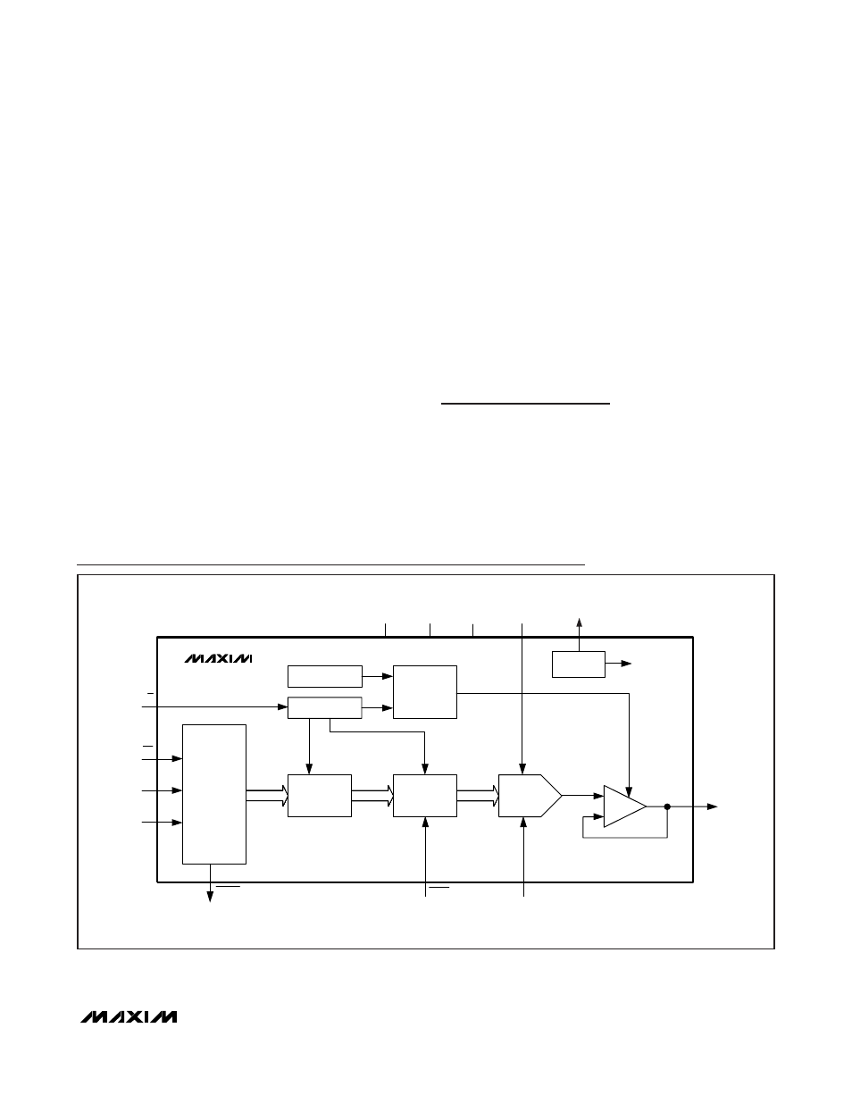
Chip Information
PROCESS: BiCMOS
MAX5138/MAX5139
Low-Power, Single, 16-/12-Bit,
Buffered Voltage-Output DACs
______________________________________________________________________________________
15
INPUT
REGISTER
12-/16-BIT
DAC
BUFFER
INTERNAL
BIAS CKT
CONTROL LOGIC
POR
POWER-DOWN
CONTROL
SERIAL-TO-
PARALLEL
CONVERTER
CS
SCLK
DIN
OUT
REFI
REFERENCE
AVDD
DVDD
AGND
READY
REFO
AGND
M/Z
LDAC
MAX5138
MAX5139
DAC
REGISTER
Functional Diagram