Max4951 sata i/sata ii bidirectional re-driver – Rainbow Electronics MAX4951 User Manual
Page 2
MAX4951
SATA I/SATA II Bidirectional Re-Driver
2
_______________________________________________________________________________________
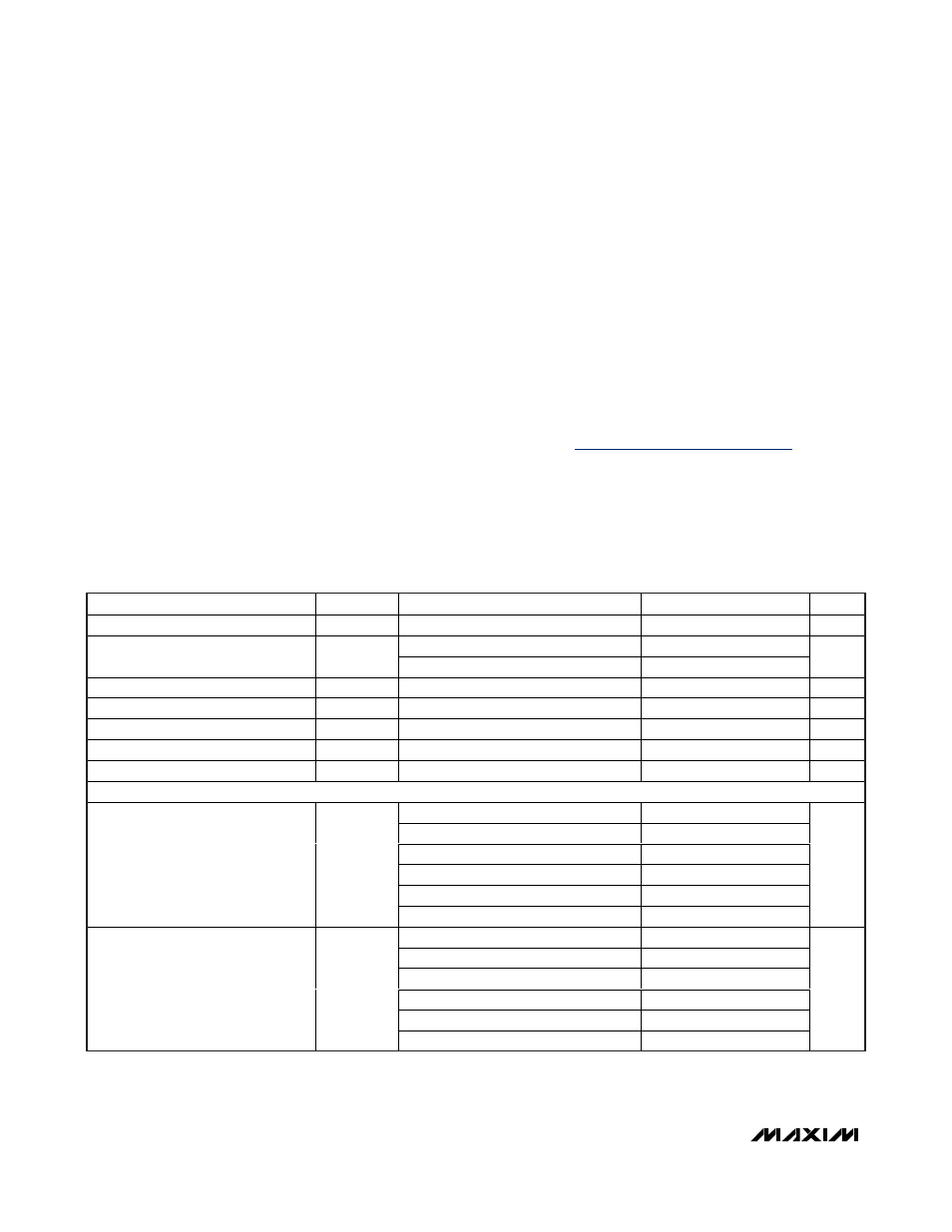
ABSOLUTE MAXIMUM RATINGS
ELECTRICAL CHARACTERISTICS
(V
CC
= +3.0V to +3.6V, C
L
= 10nF, R
L
= 50
Ω, T
A
= 0°C to +70°C, unless otherwise noted. Typical values are at V
CC
= +3.3V, T
A
= +25°C.)
(Note 3)
Stresses beyond those listed under “Absolute Maximum Ratings” may cause permanent damage to the device. These are stress ratings only, and functional
operation of the device at these or any other conditions beyond those indicated in the operational sections of the specifications is not implied. Exposure to
absolute maximum rating conditions for extended periods may affect device reliability.
(Voltages referenced to GND.)
V
CC
........................................................................-0.3V to +4.0V
HAP, HAM, DBP, DBM, EN, BA, BB
(Note 1)...................................................-0.3V to (V
CC
+ 0.3V)
Short-Circuit Output Current
(HBP, HBM, DAP, DAM) .................................................90mA
Continuous Current at Inputs
(HAP, HAM, DBP, DBM) ...............................................±30mA
Continuous Current
(EN, BA, BB) ...................................................................±5mA
Continuous Power Dissipation (T
A
= +70°C)
20-Pin TQFN (derate 25.6mW/°C above +70°C) ..... 2051mW
Junction-to-Case Thermal Resistance (
θ
JC
) (Note 2)
20-Pin TQFN...................................................................6°C/W
Junction-to-Ambient Thermal Resistance (
θ
JA
) (Note 2)
20-Pin TQFN.................................................................39°C/W
Operating Temperature Range...............................0°C to +70°C
Storage Temperature Range .............................-55°C to +150°C
Lead Temperature (soldering, 10s) .................................+300°C
PARAMETER
SYMBOL
CONDITIONS
MIN
TYP
MAX
UNITS
Operating Power-Supply Range
V
CC
3.0
3.6
V
BA = BB = V
CC
90
125
Operating Supply Current
I
CC
BA = BB = GND
70
100
mA
Standby Supply Current
I
STBY
EN = GND
7
10
mA
Single-Ended Input Resistance
Z
RX-SE-DC
40
Ω
Differential Input Resistance
Z
RX-DIFF-DC
85
100
115
Ω
Single-Ended Output Resistance
Z
TX-SE-DC
40
Ω
Differential Output Resistance
Z
TX-DIFF-DC
85
100
115
Ω
AC PERFORMANCE
f = 150MHz to 300MHz
-29
-18
f = 300MHz to 600MHz
-26
-14
f = 600MHz to 1200MHz
-22
-10
f = 1.2GHz to 2.4GHz
-18
-8
f = 2.4GHz to 3.0GHz
-15
-3
Differential Input Return Loss
(Note 4)
RL
RX-DIFF
f = 3.0GHz to 5.0GHz
-14
-1
dB
f = 150MHz to 300MHz
-5
f = 300MHz to 600MHz
-5
f = 600MHz to 1200MHz
-2
f = 1.2GHz to 2.4GHz
-2
f = 2.4GHz to 3.0GHz
-2
Common-Mode Input Return Loss
(Note 4)
RL
RX-CM
f = 3.0GHz to 5.0GHz
-1
dB
Note 1: All I/O pins are clamped by internal diodes.
Note 2: Package thermal resistances were obtained using the method described in JEDEC specification JESD51-7, using a four-layer
board. For detailed information on package thermal considerations, refer to
www.maxim-ic.com/thermal-tutorial
.