Pin description (continued), Functional diagram – Rainbow Electronics MAX16904 User Manual
Page 7
MAX16904
2.1MHz, High-Voltage,
600mA Mini-Buck Converter
_______________________________________________________________________________________
7
Pin Description (continued)
PIN
TDFN-EP TSSOP-EP
NAME
FUNCTION
5 8
OUTS
Buck Regulator Voltage-Sense Input. Bypass OUTS to PGND with a 10μF or larger X7R
ceramic capacitor.
6 11
PGOOD
Open-Drain Power-Good Output. External pullup resistor required for automatic SKIP
mode operation.
7 12
SYNC
Sync Input. SYNC allows the device to synchronize to other supplies. When
connected to GND or unconnected, SKIP mode is enabled under light loads. When
connected to a clock source or BIAS, forced PWM mode is enabled.
8
13
BIAS
+5V Internal Logic Supply. Connect a 2.2μF ceramic capacitor from BIAS to GND.
9 14
GND
Analog
Ground
10
15
EN
Enable Input. EN is high-voltage compatible. Drive EN HIGH for normal operation.
9, 10, 16
N.C.
No Connection. Not internally connected.
EP
Exposed Pad. Connect EP to PGND. Do not use EP as the only ground connection.
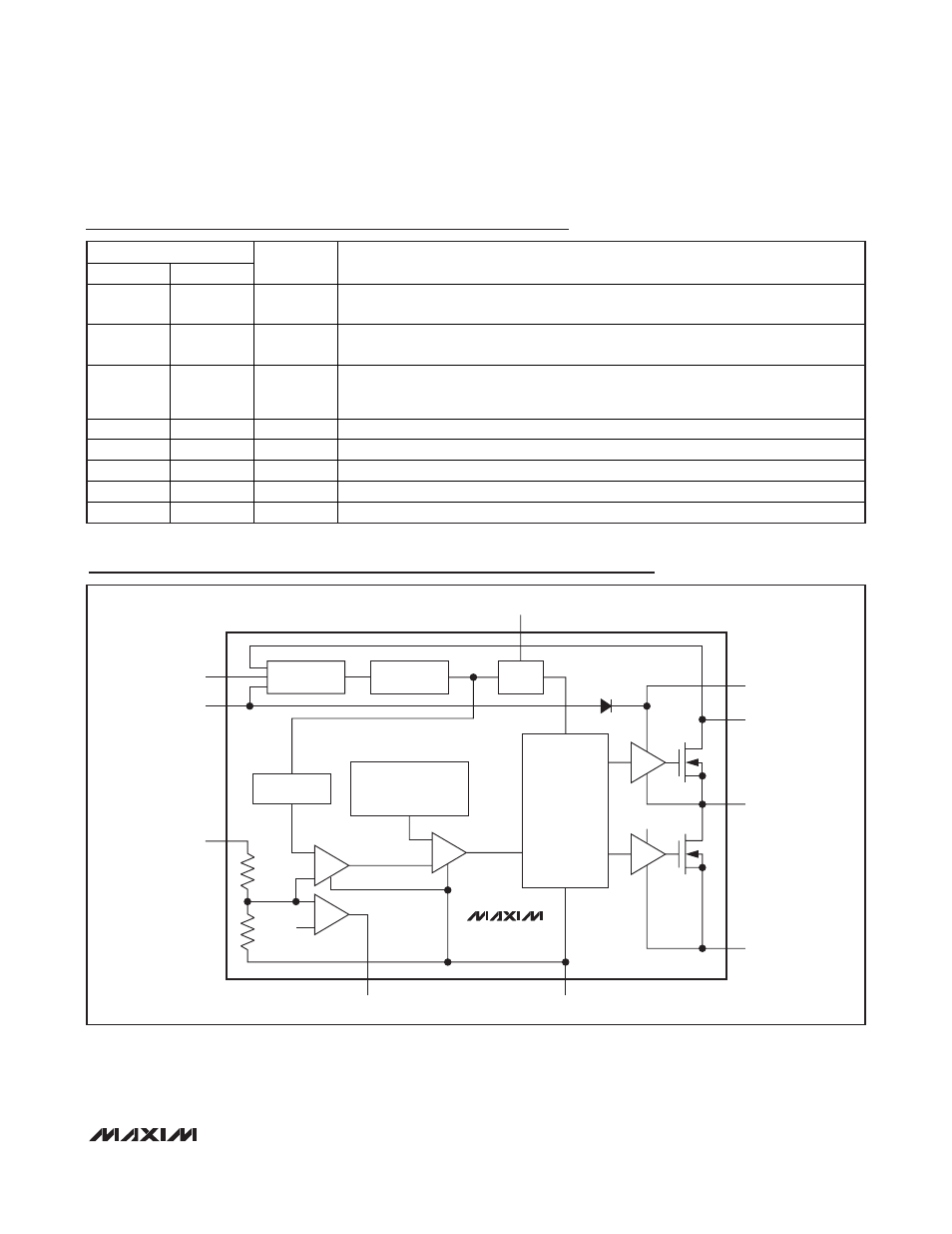
Functional Diagram
MAX16904
LSD
PWM
EAMP
COMP
HSD
BIAS
LX
PGND
BST
SUP
LOGIC
CONTROL
CURRENT-SENSE
AND
SLOPE COMPENSATION
SOFT-START
OSC
BANDGAP
GND
V
GOOD
PGOOD
OUTS
BIAS
HVLDO
SYNC
REF
EN
CLK