Typical operating characteristics (continued), Pin description, Pin configurations – Rainbow Electronics MAX16904 User Manual
Page 6
MAX16904
2.1MHz, High-Voltage,
600mA Mini-Buck Converter
6
_______________________________________________________________________________________
Typical Operating Characteristics (continued)
(V
SUP
= +14V, T
A
= +25°C, unless otherwise noted.)
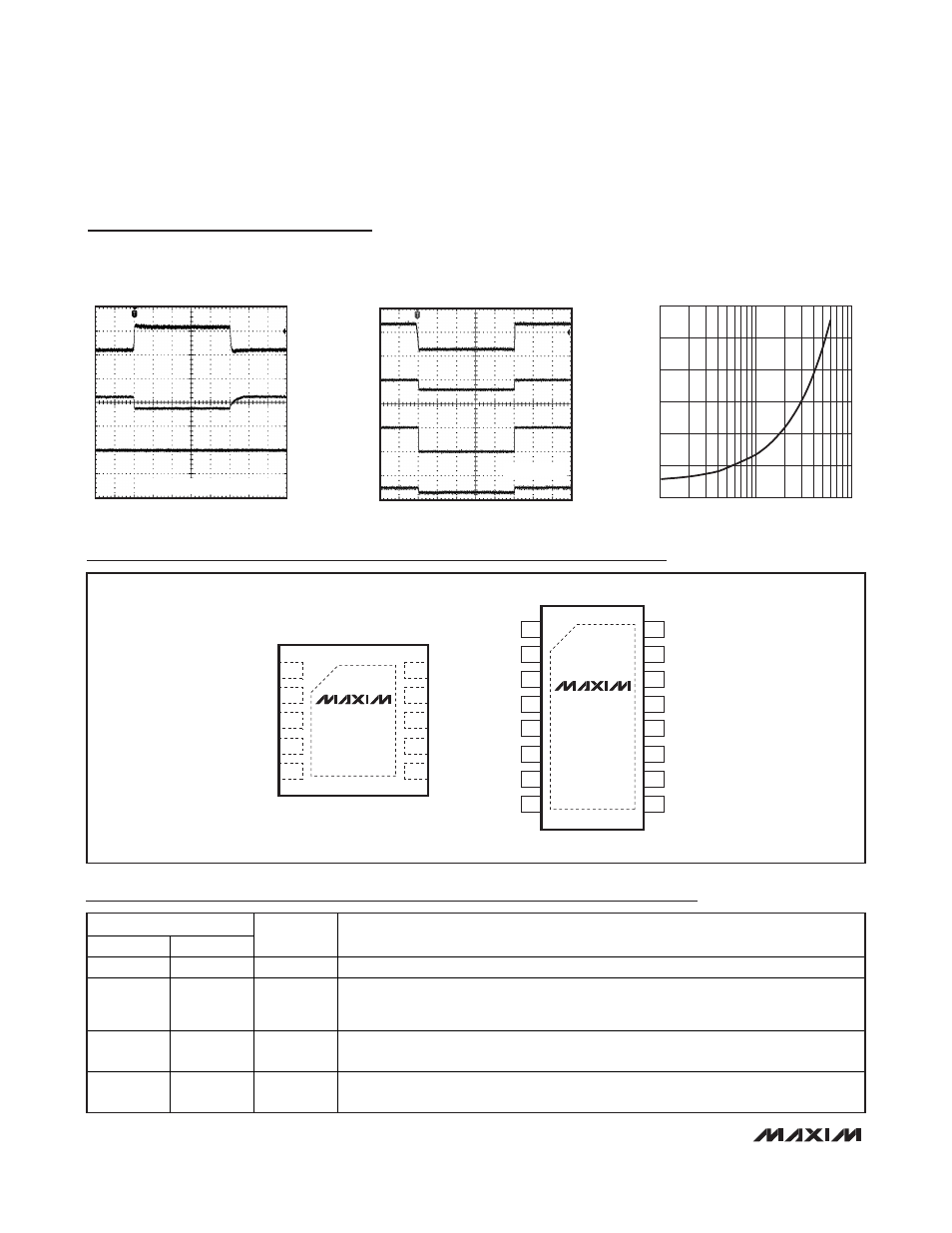
Pin Description
PIN
TDFN-EP TSSOP-EP
NAME
FUNCTION
1
1
BST
Bootstrap Capacitor for High-Side Driver (0.1μF)
2 2,
3
SUP
Voltage Supply Input. Connect a 4.7μF ceramic capacitor from SUP to PGND. Place
the capacitor very close to the SUP pin. For the TSSOP-EP package, connect both SUP
pins together for proper operation.
3 4,
5 LX
Buck Switching Node. LX is high impedance when the device is off. For the TSSOP
package, connect both LX pins together for proper operation.
4 6,
7
PGND
Power Ground. For the TSSOP-EP package, connect both PGND pins together for proper
operation.
MAX16904
+
5
6
OUTS
PGOOD
4
TOP VIEW
7
PGND
SYNC
3
8
LX
BIAS
2
9
SUP
GND
1
TDFN
10
BST
EN
EP
MAX16904
+
8
9
OUTS
N.C.
7
10
PGND
N.C.
6
11
PGND
PGOOD
3
14
SUP
GND
2
15
SUP
EN
1
16
BST
N.C.
5
12
LX
SYNC
4
TSSOP
13
LX
BIAS
EP
Pin Configurations
LOAD TRANSIENT RESPONSE
(SKIP MODE)
MAX16904 toc09
200
μs/div
5V
5V
I
LOAD
500mA/div
V
OUT
200mV/div
AC-COUPLED
PGOOD
5V/div
I
LOAD
= 100mA TO 600mA TO 100mA
UNDERVOLTAGE PULSE (COLD CRANK)
MAX16904 toc10
V
SUP
10V/div
V
OUT
5V/div
I
LOAD
1A/div
PGOOD
5V/div
14V
3.5V
10ms/div
I
LOAD
= 500mA
STANDBY CURRENT
vs. LOAD CURRENT
MAX16904 toc11
I
LOAD
(mA)
I
IN
(μ
A)
0.1
50
100
150
200
250
300
0
0.01
1