Figure 2. low-side current sensing, Ordering information, Chip information – Rainbow Electronics MAX44252 User Manual
Page 11: Functional diagrams
���������������������������������������������������������������� Maxim Integrated Products 11
MAX44251/MAX44252
20V, Ultra-Precision, Low-Noise Op Amps
Error Budget Example
When using the ICs as an ADC buffer in strain gauge
application, the temperature drift should be taken into
consideration to determine maximum input signal. A
typical strain gauge has sensitivity specification of just
2mV/V at rated out load. This means that when the strain
gauge load cell is powered with 10V, the full-scale output
voltage is 20mV. In this application, both offset voltage
and drift are critical parameters that directly affect the
accuracy of measurement. Even though offset voltage
could be calibrated out, its drift over temperature is still
a problem.
The ICs, with a typical offset drift of 5nV/°C, guarantee
that the drift over a 10°C range is only 50nV. Setting this
equal to 0.5 LSB in a 18-bit system yields a full-scale
range of 13mV. With a single 10V supply, an acceptable
closed-loop gain of 770V/V provides sufficient gain while
maintaining headroom.
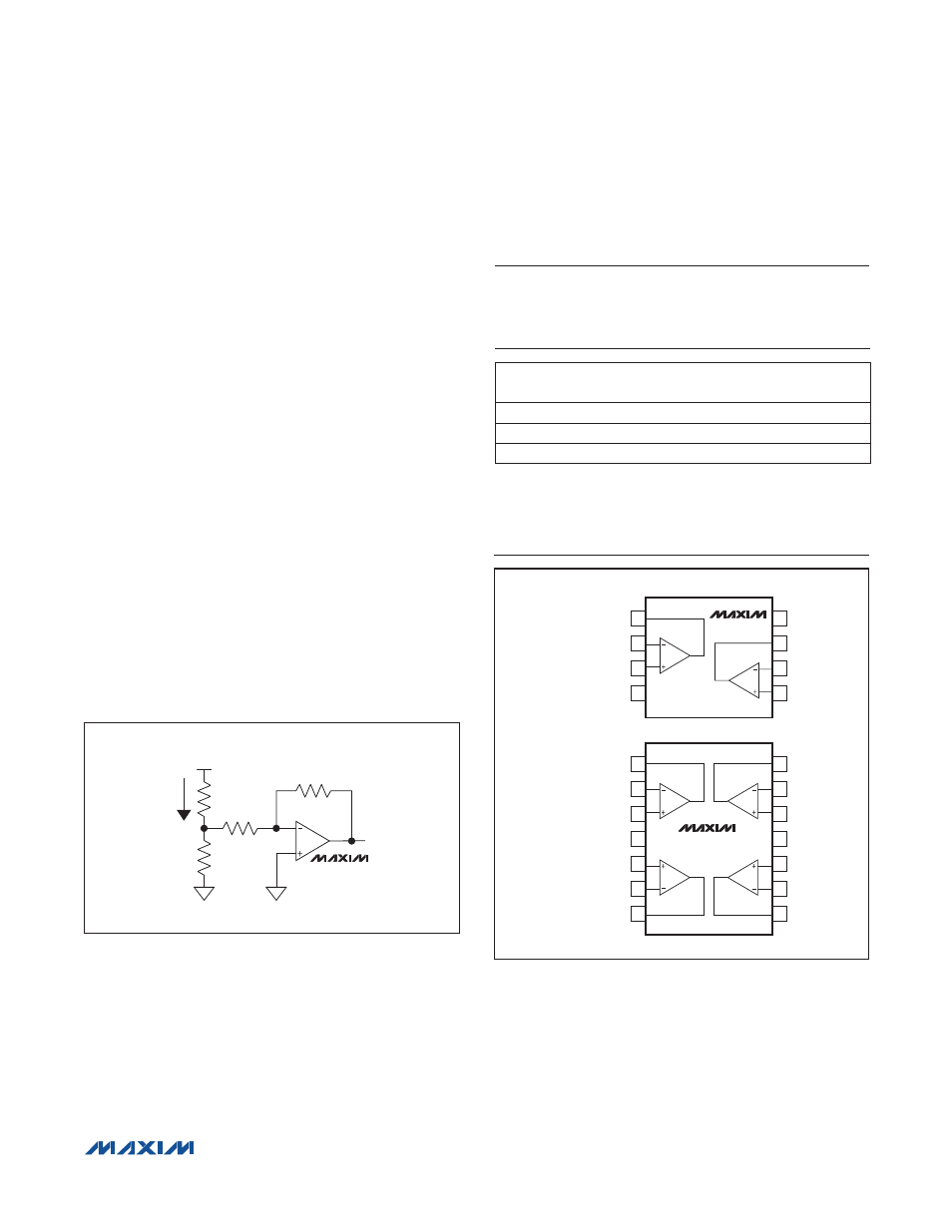
Precision Low-Side Current Sensing
The ICs’ autozero feature produces ultra-low offset
voltage and drift, making them ideal for precision cur-
rent-sensing applications. Figure 2 shows the ICs in
a low-side current-sense configuration. This circuit pro-
duces an accurate output voltage, V
OUT
equal to I
LOAD
x R
SENSE
x R
2
/R
1
.
Figure 2. Low-Side Current Sensing
Ordering Information
+Denotes a lead(Pb)-free/RoHS-compliant package.
*Future product—contact factory for availability.
Chip Information
PROCESS: BiCMOS
Functional Diagrams
PART
TEMP RANGE
PIN-
PACKAGE
TOP
MARK
MAX44251AKA+
-40NC to +125NC
8 SOT23
AERC
MAX44251AUA+
-40NC to +125NC
8 FMAX
—
MAX44252ASD+*
-40NC to +125NC
14 SOIC
—
V
SUPPLY
OUT
I
LOAD
R
SENSE
R
1
R
2
MAX44251
MAX44252
5
6
7
10
9
8
INB-
INB+
V
SS
1
2
8
7
V
DD
OUTB
INA-
INA+
OUTA
TOP VIEW
3
4
6
5
MAX44251
+
IND+
V
SS
V
DD
INB+
1
2
14
13
OUTD
IND-
INA-
INA+
INB-
OUTB
OUTA
3
4
12
11
INC+
INC-
OUTC
MAX44252
+