Detailed description, Typical operating characteristics (continued), Pin description – Rainbow Electronics MAX5365 User Manual
Page 7
Detailed Description
The MAX5363/MAX5364/MAX5365 voltage-output, 6-bit
DACs offer full 6-bit performance with less than 1LSB
integral nonlinearity error and less than 1LSB differen-
tial nonlinearity error, ensuring monotonic performance.
The devices use a simple 3-wire, SPI/QSPI/ MICROWIRE-
compatible serial interface that operates up to 10MHz.
The MAX5363/MAX5364/MAX5365 include an internal
reference, an output buffer, and three low-current shut-
down modes, making these devices ideal for low-
power, highly integrated applications. Figure 1 shows
the devices’ functional diagram.
Analog Section
The MAX5363/MAX5364MAX5365 employ a current-
steering DAC topology as shown in Figure 2. At the
core of the DAC is a reference voltage-to-current con-
verter (V/I) that generates a reference current. This current
is mirrored to 63 equally weighted current sources.
DAC switches control the outputs of these current mirrors
so that only the desired fraction of the total current-mirror
currents is steered to the DAC output. The current is
then converted to a voltage across a resistor, and this
voltage is buffered by the output buffer amplifier.
Output Voltage
Table 1 shows the relationship between the DAC code
and the analog output voltage. The 6-bit DAC code is
binary unipolar with 1LSB = (V
REF
/64). The MAX5363/
MAX5364 have a full-scale output voltage of (+2V - 1LSB)
and (+4V - 1LSB), respectively, set by the internal refer-
ences. The MAX5365 has a full-scale output voltage of
(0.9
✕
V
DD
- 1LSB).
Output Buffer
The DAC voltage output is an internally buffered unity-
gain follower that slews up to ±0.4V/µs. The output can
swing from 0 to full scale. With a 1/4FS to 3/4FS output
transition, the amplifier outputs typically settle to
1/2LSB in less than 5µs when loaded with 10k
Ω in par-
allel with 50pF. The buffer amplifiers are stable with any
MAX5363/MAX5364/MAX5365
Low-Cost, Low-Power, 6-Bit DACs with 3-Wire
Serial Interface in SOT23
_______________________________________________________________________________________
7
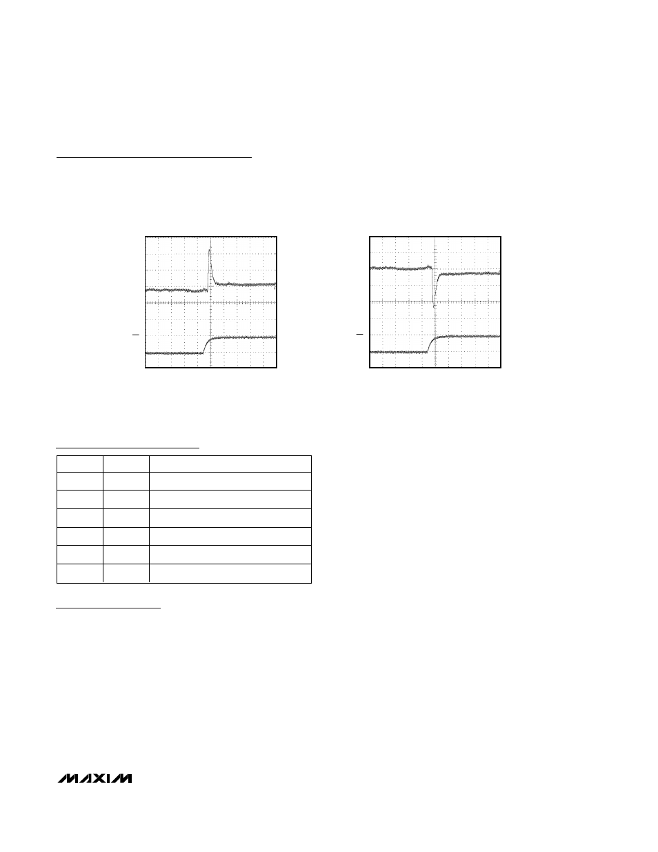
Typical Operating Characteristics (continued)
(V
DD
= +3.0V (MAX5363), V
DD
= +5.0V (MAX5364/MAX5365), T
A
= +25°C, unless otherwise noted.)
2
µs/div
MAX5363
OUTPUT SETTLING
1/4LSB STEP UP
MAX5363/4/5-22
OUT
20mV/div
AC-COUPLED
0 x 1F TO 0 x 20
CS
3V/div
MAX5363
OUTPUT SETTLING
1/4LSB STEP DOWN
MAX5363/4/5-23
OUT
20mV/div
AC-COUPLED
2
µs/div
0 x 20 TO 0 x 1F
CS
3V/div
Pin Description
PIN
NAME
FUNCTION
1
OUT
DAC Voltage Output
2
GND
Ground
3
V
DD
Power-Supply Input
4
DIN
Serial Data Input
5
SCLK
Serial Clock Input
6
CS
Chip-Select Input