Pin description – Rainbow Electronics MAX5191 User Manual
Page 7
MAX5188/MAX5191
Dual, 8-Bit, 40MHz, Current/Voltage,
Alternate-Phase Output DACs
_______________________________________________________________________________________
7
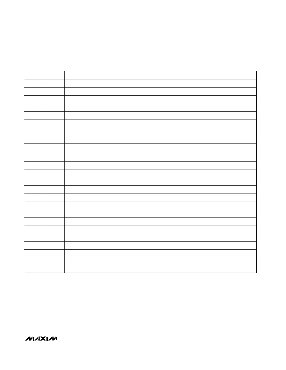
Pin Description
Data Bit D7 (MSB)
D7
21
Reference Bias Bypass, DAC2
CREF2
28
Positive Analog Output, DAC2. Current output for the MAX5188; voltage output for the MAX5191.
OUT2P
27
Negative Analog Output, DAC2. Current output for the MAX5188; voltage output for the MAX5191.
OUT2N
26
Reference Output
REFO
25
PIN
FUNCTION
NAME
Data Bit D0 (LSB)
D0
14
Data Bits D1–D6
D1–D6
15–20
Digital Supply, +2.7V to +3.3V
DV
DD
22
Reference Input
REFR
24
Clock Input
CLK
9
Not Connected. Do not connect to this pin.
N.C.
10
Active-Low Reference Enable. Connect to DGND to activate on-chip +1.2V reference.
REN
11
Digital Ground
DGND
12, 13, 23
Active-Low Chip Select
CS
8
Power-Down Select
0: Enter DAC standby mode (DACEN = DGND) or power-up DAC (DACEN = DV
DD
)
1: Enter shutdown mode
PD
7
DAC Enable, Digital Input
0: Enter DAC standby mode with PD = DGND
1: Power-up DAC with PD = DGND
X: Enter shutdown mode with PD = DV
DD
(X = don’t care)
DACEN
6
Negative Analog Output, DAC1. Current output for the MAX5188; voltage output for the MAX5191.
OUT1N
3
Analog Ground
AGND
4
Analog Positive Supply, +2.7V to +3.3V
AV
DD
5
Positive Analog Output, DAC1. Current output for the MAX5188; voltage output for the MAX5191.
OUT1P
2
1
Reference Bias Bypass, DAC1
CREF1