Applications information – Rainbow Electronics MAX5191 User Manual
Page 11
MAX5188/MAX5191
Dual, 8-Bit, 40MHz, Current/Voltage,
Alternate-Phase Output DACs
______________________________________________________________________________________
11
Timing Information
Both internal DAC cells write to their outputs in alternate
phase (Figure 4). The input latch of the first DAC
(DAC1) is loaded after the clock signal transitions high.
When the clock signal transitions low, the input latch of
the second DAC (DAC2) is loaded. The contents of the
first input latch are shifted into the DAC1 register on the
rising edge of the clock; the contents of the second
input latch are shifted into the input register of DAC2 on
the falling edge of the clock. Both outputs are updated
on alternate phases of the clock.
Outputs
The MAX5188 outputs are designed to supply 1mA full-
scale output currents into 400
Ω loads in parallel with a
capacitive load of 5pF. The MAX5191 features integrat-
ed 400
Ω resistors that restore the array currents into
proportional, differential voltages of 400mV. These dif-
ferential output voltages can then be used to drive a
balun transformer or a low-distortion, high-speed oper-
ational amplifier to convert the differential voltage into a
single-ended voltage.
Applications Information
Static and Dynamic
Performance Definitions
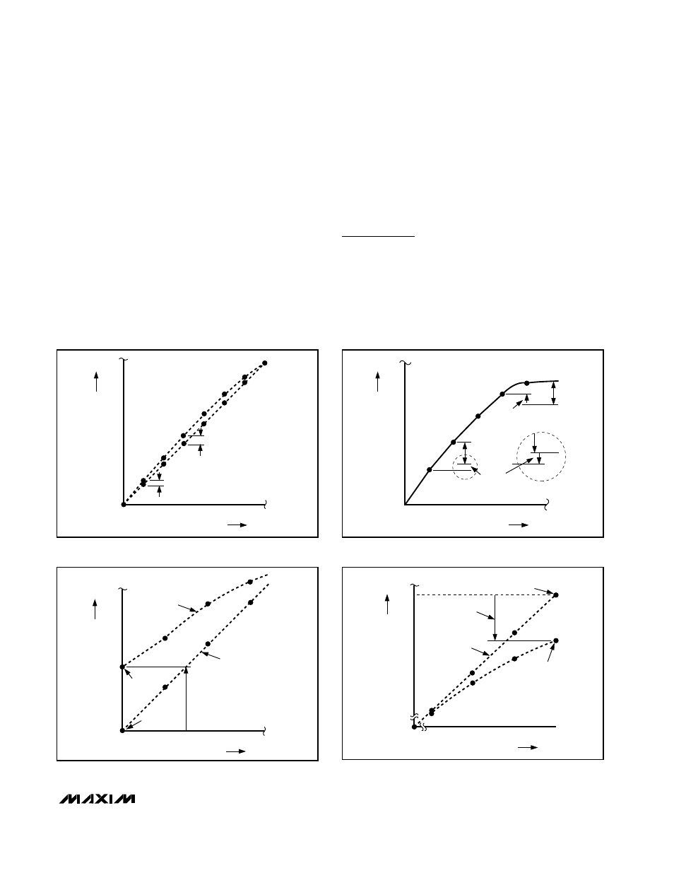
Integral Nonlinearity
Integral nonlinearity (INL) (Figure 5a) is the deviation of
the values on an actual transfer function from either a
best-straight-line fit (closest approximation to the actual
transfer curve) or a line drawn between the endpoints
0
2
1
4
3
7
6
5
000
010
001
011
100
101
110
AT STEP
011 (1/2 LSB )
AT STEP
001 (1/4 LSB )
111
DIGITAL INPUT CODE
ANALOG OUTPUT VALUE
Figure 5a. Integral Nonlinearity
Figure 5b. Differential Nonlinearity
0
2
1
4
3
6
5
000
010
001
011
100
101
DIFFERENTIAL LINEARITY
ERROR (-1/4 LSB)
DIFFERENTIAL
LINEARITY ERROR (+1/4 LSB)
1 LSB
1 LSB
DIGITAL INPUT CODE
ANALOG OUTPUT VALUE
0
2
1
3
000
010
001
011
ACTUAL
DIAGRAM
IDEAL DIAGRAM
ACTUAL
OFFSET
POINT
OFFSET ERROR
(+1 1/4 LSB)
IDEAL OFFSET
POINT
DIGITAL INPUT CODE
ANALOG OUTPUT VALUE
Figure 5c. Offset Error
Figure 5d. Gain Error
0
5
4
6
7
000
101
100
110
111
IDEAL DIAGRAM
GAIN ERROR
(-1 1/4 LSB)
IDEAL FULL-SCALE OUTPUT
ACTUAL
FULL-SCALE
OUTPUT
DIGITAL INPUT CODE
ANALOG OUTPUT VALUE