Electrical characteristics, Absolute maximum ratings – Rainbow Electronics MAX98302 User Manual
Page 2
2 ______________________________________________________________________________________
MAX98302
Stereo 2.4W Class D Amplifier
Stresses beyond those listed under “Absolute Maximum Ratings” may cause permanent damage to the device. These are stress ratings only, and functional
operation of the device at these or any other conditions beyond those indicated in the operational sections of the specifications is not implied. Exposure to absolute
maximum rating conditions for extended periods may affect device reliability.
PVDD to PGND .......................................................... -0.3V to 6V
All Other Pins to PGND ..........................-0.3V to (PVDD + 0.3V)
Continuous Current into PVDD, PGND,
OUTL_, OUTR_ .......................................................... Q600mA
Continuous Input Current (all other pins) ........................ Q20mA
Duration of Short Circuit Between OUTL_,
OUTR_ to PVDD or PGND .....................................Continuous
Duration of Short Circuit Between OUTL+ to OUTL-,
OUTR+ to OUTR- ..................................................Continuous
Continuous Power Dissipation for Single Layer Board (T
A
= +70NC)
14-Pin TDFN (derate 18.5mW/NC above +70NC) ....1481.5mW
14-Pin TDFN B
JA
(Note 1) ............................................54NC/W
14-Pin TDFN B
JC
(Note 1) ..............................................8NC/W
Continuous Power Dissipation for Multilayer Board (T
A
= +70NC)
14-Pin TDFN (derate 24.4mW/NC above +70NC) ....1951.2mW
14-Pin TDFN B
JA
(Note 1) ............................................41NC/W
14-Pin TDFN B
JC
(Note 1) ..............................................8NC/W
Junction Temperature .....................................................+150NC
Operating Temperature Range .......................... -40NC to +85NC
Storage Temperature Range ............................ -65NC to +150NC
Lead Temperature (soldering, 10s) ................................+300NC
Soldering Temperature (reflow) ......................................+260NC
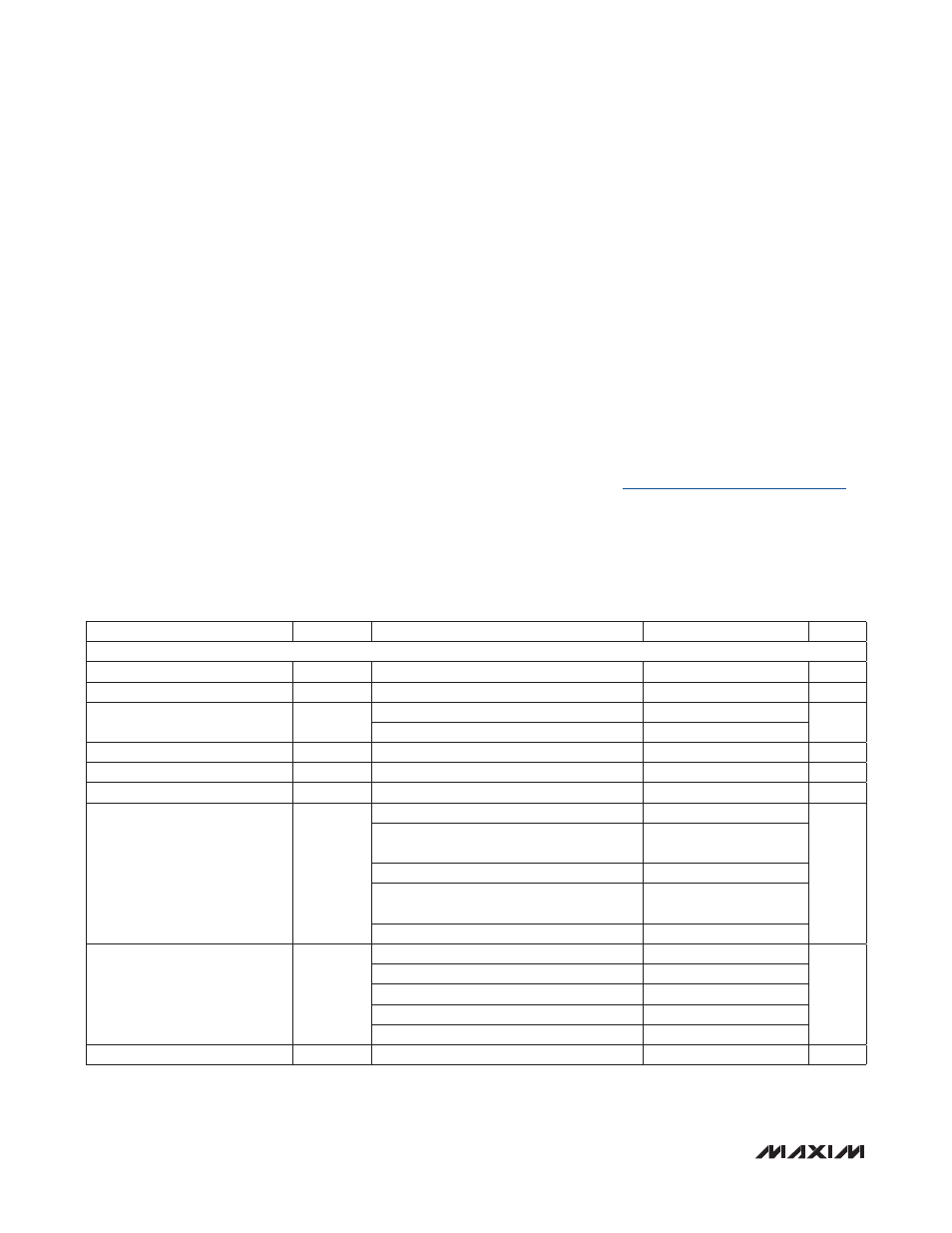
ELECTRICAL CHARACTERISTICS
(V
PVDD
= V
SHDN
= 5.0V, V
PGND
= 0V, AV = 12dB (GAIN = PVDD), R
L
= J, R
L
connected between OUT_+ to OUT_-, 20Hz to 22kHz
AC measurement bandwidth, T
A
= T
MIN
to T
MAX
, unless otherwise noted. Typical values are at T
A
= +25NC.) (Notes 2, 3)
ABSOLUTE MAXIMUM RATINGS
Note 1: Package thermal resistances were obtained using the method described in JEDEC specification JESD51-7, using a four-
layer board. For detailed information on package thermal considerations, refer to
www.maxim-ic.com/thermal-tutorial
.
PARAMETER
SYMBOL
CONDITIONS
MIN
TYP
MAX
UNITS
AMPLIFIER CHARACTERISTICS
Supply Voltage Range
V
PVDD
Inferred from PSRR test
2.6
5.5
V
Undervoltage Lockout
UVLO
2.5
V
Quiescent Supply Current
I
DD
V
PVDD
= 5.0V, T
A
= +25NC
2.25
3.4
mA
V
PVDD
= 3.7V
1.65
Shutdown Supply Current
I
SHDN
V
SHDN
= 0V, T
A
= +25NC
0.1
10
F
A
Turn-On Time
t
ON
3.7
10
ms
Bias Voltage
V
BIAS
1.3
V
Voltage Gain
A
V
Connect GAIN to PGND
17.5
18
18.5
dB
Connect GAIN to PGND through 100kI
±5%
resistor
14.5
15
15.5
Connect GAIN to PVDD
11.5
12
12.5
Connect GAIN to PVDD through 100kI
±5%
resistor
8.5
9
9.5
GAIN unconnected
5.5
6
6.5
Input Resistance
R
IN
A
V
= 18dB
14
20
kI
A
V
= 15dB
14
20
A
V
= 12dB
14
20
A
V
= 9dB
19
28
A
V
= 6dB
26
40
Output Offset Voltage
V
OS
T
A
= +25NC (Note 4)
±4
±20
mV