Rainbow Electronics MAX5184 User Manual
Page 2
MAX5181/MAX5184
10-Bit, 40MHz, Current/Voltage-Output DACs
2
_______________________________________________________________________________________
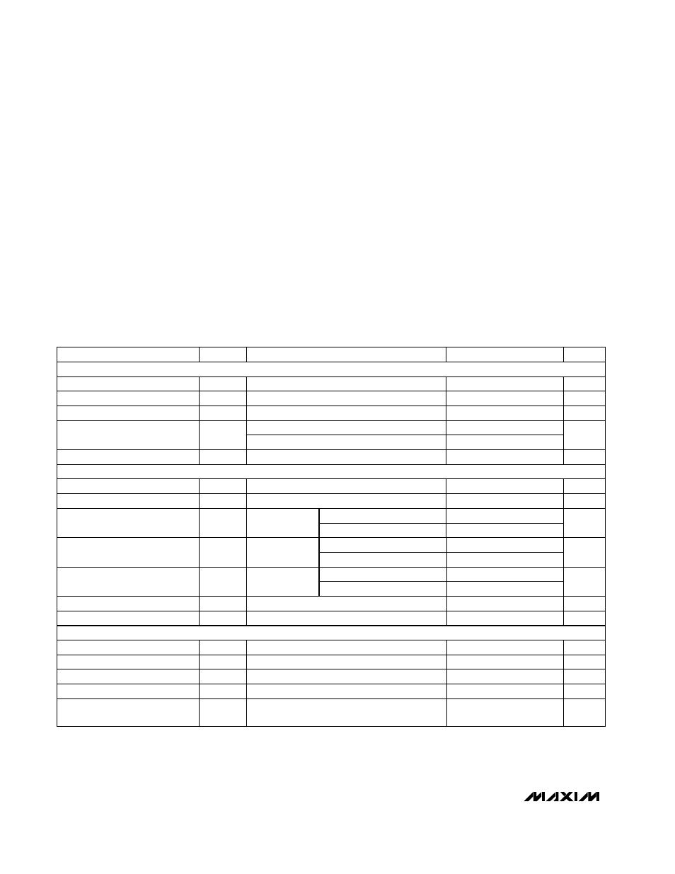
ABSOLUTE MAXIMUM RATINGS
ELECTRICAL CHARACTERISTICS
(AV
DD
= DV
DD
= +3V ±10%, AGND = DGND = 0, f
CLK
= 40MHz, I
FS
= 1mA, 400
Ω differential output, C
L
= 5pF, T
A
= T
MIN
to T
MAX
,
unless otherwise noted. Typical values are at T
A
= +25°C.)
Stresses beyond those listed under “Absolute Maximum Ratings” may cause permanent damage to the device. These are stress ratings only, and functional
operation of the device at these or any other conditions beyond those indicated in the operational sections of the specifications is not implied. Exposure to
absolute maximum rating conditions for extended periods may affect device reliability.
AV
DD
, DV
DD
to AGND, DGND .................................-0.3V to +6V
Digital Inputs to DGND.............................................-0.3V to +6V
OUTP, OUTN, CREF to AGND .................................-0.3V to +6V
V
REF
to AGND ..........................................................-0.3V to +6V
AGND to DGND.....................................................-0.3V to +0.3V
AV
DD
to DV
DD
.................................................................... ±3.3V
Maximum Current into Any Pin............................................50mA
Continuous Power Dissipation (T
A
= +70°C)
24-Pin QSOP (derate 9.50mW/°C above +70°C) ........762mW
Operating Temperature Range
MAX518_BEEG ................................................-40°C to +85°C
Storage Temperature Range .............................-65°C to +150°C
Lead Temperature (soldering, 10s) .................................+300°C
MAX5181 only
MAX5181 only
DACEN = 0, MAX5181 only
All 0s to all 1s
To ±0.5LSB error band
Guaranteed monotonic
MAX5181
(Note 1)
CONDITIONS
Ω
400
R
L
DAC External Output Resistor
Load
mA
0.5
1
1.5
I
FS
Full-Scale Output Current
µA
-1
1
Output Leakage Current
V
-0.3
0.8
Voltage Compliance of Output
mV
400
V
FS
Full-Scale Output Voltage
pA/
√Hz
10
Output Noise
LSB
-2
±0.5
+2
INL
Integral Nonlinearity
Bits
10
N
Resolution
nVs
50
Clock and Data Feedthrough
dBc
72
SFDR
Spurious-Free Dynamic Range
to Nyquist
pVs
10
Glitch Impulse
ns
25
Output Settling Time
LSB
-1
±0.5
1
DNL
Differential Nonlinearity
-2
+2
Zero-Scale Error
LSB
-40
±15
+40
Full-Scale Error
UNITS
MIN
TYP
MAX
SYMBOL
PARAMETER
57
70
-68
-63
dB
-70
THD
Total Harmonic Distortion
to Nyquist
56
59
dB
61
SNR
Signal-to-Noise Ratio to Nyquist
f
OUT
= 550kHz
f
OUT
= 2.2MHz, T
A
= +25°C
f
OUT
= 550kHz
f
OUT
= 2.2MHz, T
A
= +25°C
f
OUT
= 550kHz
f
OUT
= 2.2MHz, T
A
= +25°C
f
CLK
= 40MHz
f
CLK
= 40MHz
f
CLK
= 40MHz
DYNAMIC PERFORMANCE
STATIC PERFORMANCE
ANALOG OUTPUT
MAX5184
-8
+8
LSB