Electrical characteristics, Absolute maximum ratings – Rainbow Electronics MAX8848Z User Manual
Page 2
High-Performance Negative Charge Pump
for 7 White LEDs in 3mm x 3mm Thin QFN
MAX8848Y/MAX8848Z
2 ______________________________________________________________________________________
Stresses beyond those listed under “Absolute Maximum Ratings” may cause permanent damage to the device. These are stress ratings only, and functional
operation of the device at these or any other conditions beyond those indicated in the operational sections of the specifications is not implied. Exposure to absolute
maximum rating conditions for extended periods may affect device reliability.
IN to GND .............................................................-0.3V to +6.0V
IN to NEG .............................................................-0.3V to +6.0V
NEG, C2N to GND ..................................................-6V to +0.3V
C1P, C2P, CPWM, ENA, ENB to GND .......-0.3V to (V
IN
+ 0.3V)
C2P to C1N ................................................-0.3V to (V
IN
+ 0.3V)
LED_, C1N, C2N, ENA, ENB to NEG .........-0.3V to (V
IN
+ 0.3V)
Continuous Power Dissipation (T
A
= +70°C)
16-Pin Thin QFN Multilayer PCB
(derate 20.8mW/°C above +70°C)..........................1666.7mW
Junction-to-Case Thermal Resistance (
θ
JC
) (Note 1) .....10°C/W
Junction-to-Ambient Thermal Resistance (
θ
JA
) (Note 1)
Multilayer PCB ..............................................................48°C/W
Operating Temperature Range .......................... -40°C to +85°C
Junction Temperature .....................................................+150°C
Storage Temperature Range ............................ -65°C to +150°C
Lead Temperature (soldering, 10s) ................................+300°C
Soldering Temperature (reflow) ......................................+260°C
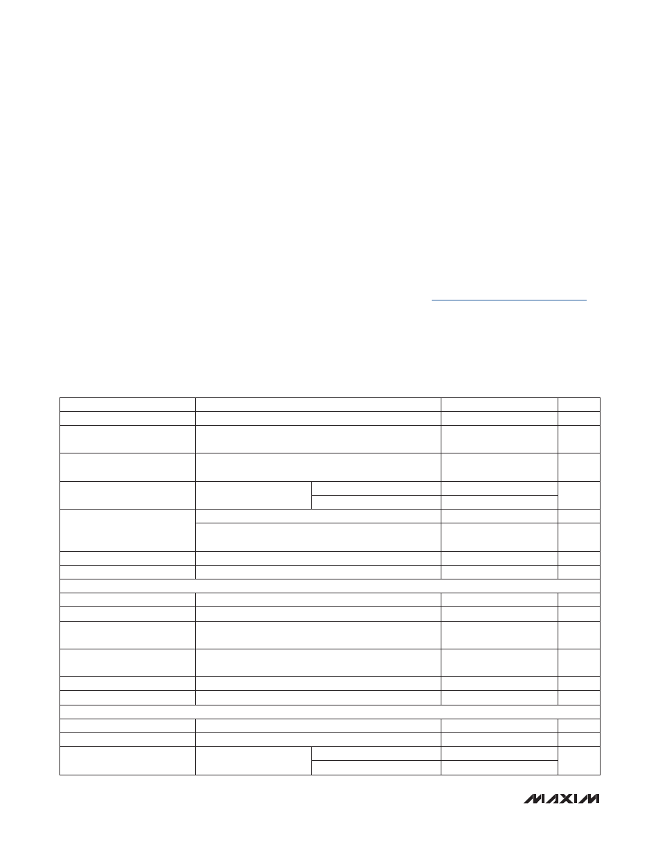
ELECTRICAL CHARACTERISTICS
(V
IN
= 3.6V, V
GND
= 0V, T
A
= -40°C to +85°C, unless otherwise noted. Typical values are at T
A
= +25°C.) (Note 2)
ABSOLUTE MAXIMUM RATINGS
Note 1: Package thermal resistances were obtained using the method described in JEDEC specification JESD51-7, using a four-
layer board. For detailed information on package thermal considerations, refer to
.
PARAMETER
CONDITIONS
MIN
TYP
MAX
UNITS
IN Operating Voltage
2.7
5.5
V
Undervoltage Lockout (UVLO)
Threshold
V
IN
rising
2.35
2.45
2.55
V
Undervoltage Lockout
Hysteresis
100
mV
IN Shutdown Supply Current
V
EN
_ = 0V, all outputs off
T
A
= +25NC
0.4
2.5
F
A
T
A
= +85NC
0.4
IN Operating Supply Current
Charge pump inactive, 2 LEDs enabled at 0.1mA setting
120
150
F
A
Charge pump active, 1MHz switching, all LEDs enabled
at 0.1mA setting
1.6
mA
Thermal Shutdown Threshold
+160
N
C
Thermal Shutdown Hysteresis
20
N
C
PWM DIMMING CONTROL (MAX8848Z)
PWM Low-Level Input
0.4
V
PWM High-Level Input
1.4
V
EN_ PWM Input Signal
Frequency Range
C
CPWM
= 0.22FF
0.2
200
kHz
PWM Dimming Filter Corner
Frequency
C
CPWM
= 0.22FF
2
Hz
Current Dimming Range
Duty cycle = 0 to 100%
0
24
mA
PWM Dimming Resolution
1% P duty cycle P 100%
0.24
mA/%
SERIAL-PULSE LOGIC (MAX8848Y)
EN_ Logic Input High Voltage
1.4
V
EN_ Logic Input Low Voltage
0.4
V
EN_ Logic-Input Current
V
IL
= 0V or V
IH
= 5.5V
T
A
= +25NC
-1
0.01
+1
F
A
T
A
= +85NC
0.1