Pin description, Typical operating characteristics (continued) – Rainbow Electronics MAX15041 User Manual
Page 7
MAX15041
Low-Cost, 3A, 4.5V to 28V Input, 350kHz, PWM
Step-Down DC-DC Regulator with Internal Switches
_______________________________________________________________________________________
7
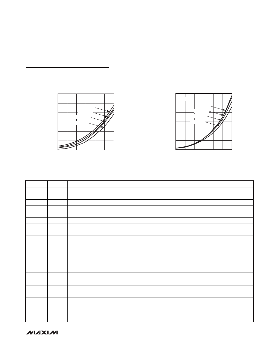
DEVICE POWER DISSIPATION
vs. LOAD CURRENT
MAX15041 toc22
LOAD CURRENT (A)
POWER DISSIPATION (W)
2.5
2.0
1.5
1.0
0.5
0.5
1.0
1.5
2.0
2.5
3.0
0
0
3.0
V
OUT
= 3.3V
V
OUT
= 2.5V
V
OUT
= 1.8V
V
OUT
= 1.2V
V
IN
= 12V
DEVICE POWER DISSIPATION
vs. LOAD CURRENT
MAX15041 toc23
LOAD CURRENT (A)
POWER DISSIPATION (W)
2.5
2.0
1.5
1.0
0.5
0.5
1.0
1.5
2.0
2.5
3.0
0
0
3.0
V
OUT
= 3.3V
V
OUT
= 2.5V
V
OUT
= 1.8V
V
OUT
= 1.2V
V
IN
= 5V
Pin Description
PIN
NAME
FUNCTION
1
V
DD
Internal LDO 5V Output. Supply input for the internal analog core. Bypass with a ceramic capacitor of at
least 1µF to SGND. See Figure 3.
2
PGOOD
Power-Good Open-Drain Output. PGOOD goes low if FB is below 545mV.
3
EN
Enable Input. EN is a digital input that turns the regulator on and off. Drive EN high to turn on the regulator.
Connect to IN for always-on operations.
4
COMP
Voltage Error-Amplifier Output. Connect the necessary compensation network from COMP to SGND.
5
FB
Feedback Input. Connect FB to the center tap of an external resistor-divider from the output to SGND to set
the output voltage from 0.606V to 90% of V
IN
.
6
SS
Soft-Start Input. Connect a capacitor from SS to SGND to set the soft-start time (see the Setting the Soft-
Start Time section).
7
SGND
Analog Ground. Connect to PGND plane at one point near the input bypass capacitor return terminal.
8
I.C.
Internally Connected. Connect to SGND.
9
BST
High-Side MOSFET Driver Supply. Bypass BST to LX with a 10nF capacitor. Connect an external diode
(see the Diode Selection section) from V
DD
to BST.
10, 11, 12
LX
Inductor Connection. Connect the LX pin to the switched side of the inductor. LX is high impedance when
the IC is in shutdown mode, thermal shutdown mode, or V
DD
is below the UVLO threshold.
13, 14
PGND
Power Ground. Connect to the SGND PCB copper plane at one point near the input bypass capacitor
return terminal.
15, 16
IN
Input Power Supply. Input supply range is from 4.5V to 28V. Bypass with a ceramic capacitor of at least
22µF to PGND.
—
EP
Exposed Pad. Connect to SGND externally. Solder the exposed pad to a large contiguous copper plane to
maximize thermal performance.
Typical Operating Characteristics (continued)
(V
IN
= 12V, V
OUT
= 3.3V, C
VDD
= 1µF, C
IN
= 22µF, T
A
= +25°C, circuit of Figure 3 (see Table 1 for values), unless otherwise specified.)