Rainbow Electronics MAX16999 User Manual
Page 2
MAX16999
Ultra-Low Output Voltage, Low-Quiescent-Current
Linear Regulator for High-Temperature Applications
2
_______________________________________________________________________________________
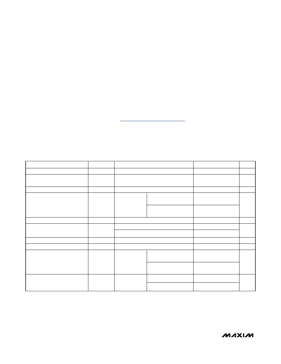
ABSOLUTE MAXIMUM RATINGS
DC ELECTRICAL CHARACTERISTICS
(For devices with V
OUT
≤ 1.5V, V
IN
= 3.3V. For devices with V
OUT
> 1.5V, V
IN
= 5V. EN = IN, T
J
= -40°C to +125°C, C
IN
= 1µF, C
OUT
= 4.7µF, C
CRES
= 1000pF, unless otherwise noted. Typical values are at T
A
= +25°C.) (Note 1)
Stresses beyond those listed under “Absolute Maximum Ratings” may cause permanent damage to the device. These are stress ratings only, and functional
operation of the device at these or any other conditions beyond those indicated in the operational sections of the specifications is not implied. Exposure to
absolute maximum rating conditions for extended periods may affect device reliability.
IN, RESET to GND .................................................-0.3V to +6.0V
OUT, CRES, EN to GND ..............................-0.3V to (V
IN
+ 0.3V)
Output Short-Circuit Duration.....................................Continuous
Continuous Power Dissipation (T
A
= +70°C) (Note 1)
(derate 10.3mW/°C above +70°C)
8-Pin µMAX (single-layer PCB) ..................................824.7mW
(derate 12.9mW/°C above +70°C)
8-Pin µMAX (multilayer PCB)....................................1030.9mW
Package Junction-to-Case Thermal Resistance (
θ
JC
) ......4.8°C/W
Package Junction-to-Ambient Thermal Resistance (
θ
JA
)
(single-layer PCB) ........................................................97°C/W
Package Junction-to-Ambient Thermal Resistance (
θ
JA
)
(multilayer PCB) ........................................................77.6°C/W
Operating Temperature Range .........................-40°C to +125°C
Junction Temperature ......................................................+150°C
Storage Temperature Range .............................-60°C to +150°C
Lead Temperature (soldering, 10s) .................................+300°C
PARAMETER
SYMBOL
CONDITIONS
MIN
TYP
MAX
UNITS
IN Operating Voltage
V
IN
2.5
5.5
V
IN Undervoltage-Lockout (UVLO)
Threshold
V
UVLO
V
IN
rising
1.94
2.2
V
IN UVLO Hysteresis
45
mV
V
OUT
≤ 1.5V,
I
OUT
= 1mA to 80mA
-2.5
+2.5
Output-Voltage Accuracy
V
IN
= V
OUT
+ 2V
V
OUT
> 1.5V,
I
OUT
= 1mA to 100mA
-2.5
+2.5
%
Current Limit
I
LIM
OUT = GND
105
150
mA
I
OUT
= 100µA
13
20
Ground Current
I
Q
I
OUT
= 100mA
23
µA
Dropout Voltage
V
IN
- V
OUT
I
OUT
= 80mA, V
OUT
= 3.3V (Note 2)
0.035
0.1
V
Load Regulation
ΔV
OUT
/
ΔI
OUT
I
OUT
= 1mA to 80mA
0.1
mV/mA
V
OUT
< 1V,
2.5V < V
IN
< 5.5V
0.4
Line Regulation
ΔV
OUT
/
ΔV
IN
I
OUT
= 80mA
V
OUT
≥ 1V, (V
OUT
+
1.5V) < V
IN
< 5.5V
1.8
mV/V
f = 100Hz
70
Power-Supply Rejection Ratio
PSRR
I
OUT
= 10mA,
500mV
P-P,
V
IN
-
V
OUT
> 1.5V
f = 100kHz
40
dB
Note 1: Package thermal resistances were obtained using the method described in JEDEC specifications. For detailed information
on packaging thermal considerations, refer to
www.maxim-ic.com/thermal-tutorial
.