Rainbow Electronics MAX5929 User Manual
Page 21

The maximum inrush current in this case is:
Figure 6 shows the waveforms and timing diagrams for
a startup transient with current regulation (see the
Typical Operating Characteristics). When operating
under this condition, an external gate capacitor is
not required.
ON Comparators
The ON comparators control the on/off function of the
MAX5927/MAX5929. ON_ is also used to reset the fault
latch (latch mode). Pull V
ON_
low for 100µs, t
UNLATCH
,
to reset the shutdown latch. ON_ also programs the
UVLO threshold (see Figure 10). A resistive-divider
between V
IN_
, V
ON_
, and GND sets the user program-
mable turn-on voltage. In power-sequencing mode, an
RC circuit can be used at ON_ to set the delay timing
(see Figure 11).
Using the MAX5927/MAX5929 on the
Backplane
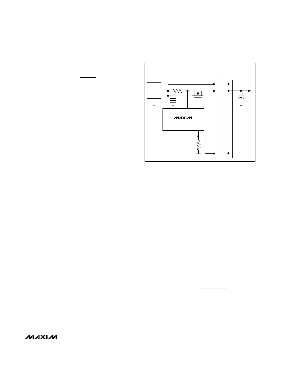
Using the MAX5927/MAX5929 on the backplane allows
multiple cards with different input capacitance to be
inserted into the same slot even if the card does not
have on-board hot-swap protection. The startup period
can be triggered if IN_ is connected to ON_ through a
trace on the card (Figure 12).
Input Transients
The voltage at IN1, IN2, IN3, or IN4 must be above V
UVLO
during inrush and fault conditions. When a short-circuit
condition occurs on the board, the fast comparator trips
cause the external MOSFET gates to be discharged at
50mA according to the mode of operation (see the Mode
section). The main system power supply must be able to
sustain a temporary fault current, without dropping below
the UVLO threshold of 2.45V, until the external MOSFET is
completely off. If the main system power supply collapses
below UVLO, the MAX5927/MAX5929 force the device to
restart once the supply has recovered. The MOSFET is
turned off in a very short time resulting in a high di/dt. The
backplane delivering the power to the external card must
have low inductance to minimize voltage transients
caused by this high di/dt.
MOSFET Thermal Considerations
During normal operation, the external MOSFETs dissi-
pate little power. The MOSFET R
DS(ON)
is low when the
MOSFET is fully enhanced. The power dissipated in nor-
mal operation is P
D
= I
LOAD
2
x R
DS(ON)
. The most
power dissipation occurs during the turn-on and turn-off
transients when the MOSFETs are in their linear regions.
Take into consideration the worst-case scenario of a
continuous short-circuit fault, consider these two cases:
1) The single turn-on with the device latched after a
fault: MAX5927 (LATCH = high or floating) or
MAX5929L.
2) The continuous autoretry after a fault: (MAX5927
(LATCH = low) or MAX5929A.
MOSFET manufacturers typically include the package
thermal resistance from junction to ambient (R
θJA
) and
thermal resistance from junction to case (R
θJC
), which
determines the startup time and the retry duty cycle (d
= t
START
/(t
START
+ t
RETRY
). Calculate the required tran-
sient thermal resistance with the following equation:
where I
START
= V
SU,TH
/ R
SENSE
.
Z
T
T
V
I
JA MAX
JMAX
A
IN
START
θ (
)
≤
−
×
I
V
R
INRUSH
FC TH
SENSE
=
,
MAX5927/MAX5929
Low-Voltage, Quad, Hot-Swap
Controllers/Power Sequencers
______________________________________________________________________________________
21
Figure 12. Using the MAX5927/MAX5929 on a Backplane
ON_
IN_
GATE_
V
IN
V
OUT
SENSE_
MAX5927
MAX5929
C
BOARD
BACKPLANE
POWER
SUPPLY
REMOVABLE CARD
WITH NO HOT-INSERTION
PROTECTION
