Rainbow Electronics MAX5929 User Manual
Page 19

Startup Sequence
There are two ways of completing the startup
sequence. Case A describes a startup sequence that
slowly turns on the MOSFETs by limiting the gate
charge. Case B uses the current-limiting feature and
turns on the MOSFETs as fast as possible while still
preventing a high inrush current. The output voltage
ramp-up time (t
ON
) is determined by the longer of the
two timings, case A and case B. Set the startup timer
(t
START
) to be longer than t
ON
to guarantee enough
time for the output voltage to settle.
Case A: Slow Turn-On (Without Current Limit)
There are two ways to turn on the MOSFETs without
reaching the fast-comparator current limit:
• If the board capacitance (C
BOARD
) is small, the
inrush current is low.
• If the gate capacitance is high, the MOSFETs turn
on slowly.
In both cases, the turn-on time is determined only by
the charge required to enhance the MOSFET. The
small 100µA gate-charging current effectively limits
the output voltage dV/dt. Connecting an external
capacitor between GATE and GND extends the turn-
on time. The time required to charge/discharge a
MOSFET is as follows:
where:
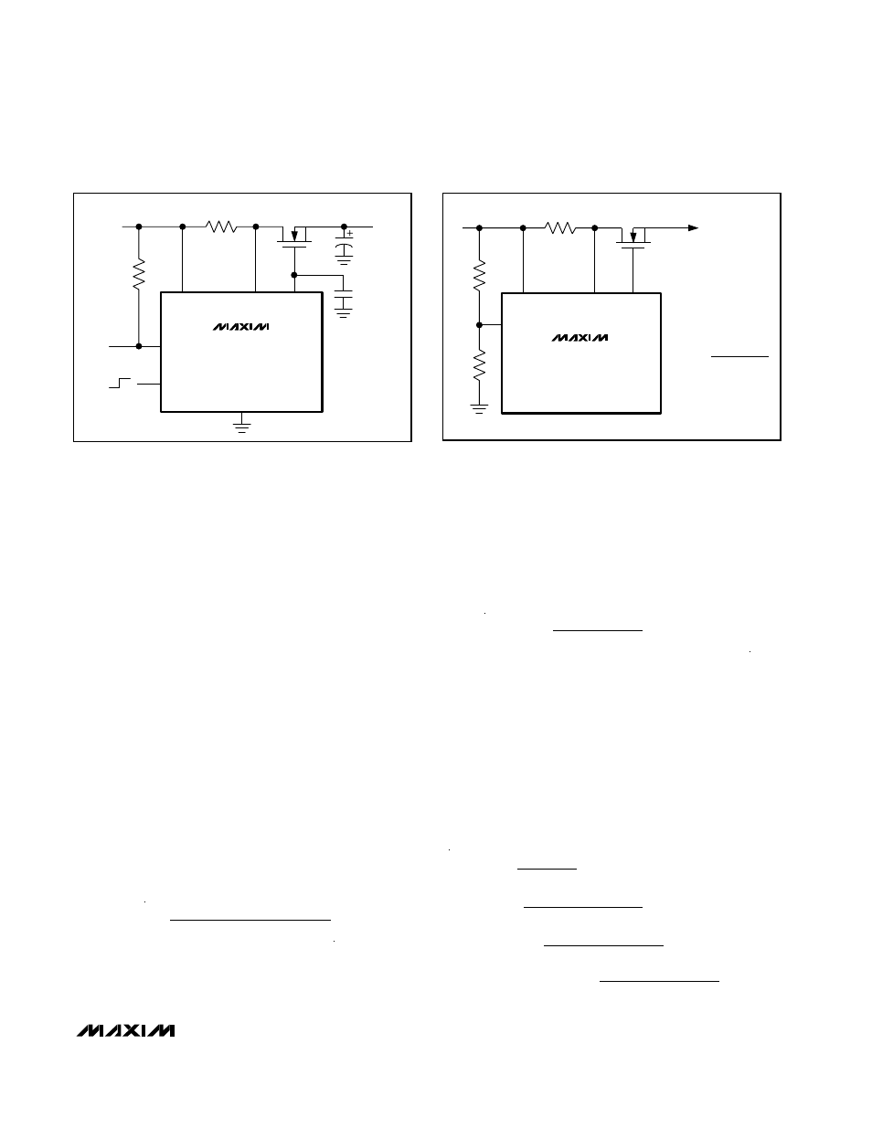
C
GATE
is the external gate to ground capacitance
(Figure 9),
∆V
GATE
is the change in gate charge,
Q
GATE
is the MOSFET total gate charge,
I
GATE
is the gate-charging/discharging current.
In this case, the inrush current depends on the MOSFET
gate-to-drain capacitance (C
rss
) plus any additional
capacitance from GATE to GND (C
GATE
), and on any
load current (I
LOAD
) present during the startup period.
Example: Charging and discharging times using the
Fairchild FDB7030L MOSFET
If V
IN1
= 5V then GATE1 charges up to 10.4V (V
IN1
+
V
DRIVE
), therefore
∆V
GATE
= 10.4V. The manufacturer’s
data sheet specifies that the FDB7030L has approxi-
mately 60nC of gate charge and C
rss
= 600pF. The
MAX5927/MAX5929 have a 100µA gate-charging cur-
rent and a 3mA/50mA normal/strong discharging cur-
rent. C
BOARD
= 6µF and the load does not draw any
current during the startup period. With no gate capaci-
tor, the inrush current, charge, and discharge times are:
I
F
pF
A
A
I
V
nC
A
ms
t
V
nC
mA
ms
t
V
nC
mA
s
INRUSH
CHARGE
DISCHARGE
DISCHARGE STRONG
=
µ
+
Ч
+
=
=
Ч
+
µ
=
=
Ч
+
=
=
Ч
+
=
6
600
0
100
0
1
0
10 4
60
100
0 6
0
10 4
60
3
0 02
0
10 4
60
50
1 2
.
.
.
.
.
.
(
)
µ
µ
I
C
C
C
I
I
INRUSH
BOARD
rss
GATE
GATE
LOAD
=
+
×
+
t
C
V
Q
I
GATE
GATE
GATE
GATE
=
×
+
∆
MAX5927/MAX5929
Low-Voltage, Quad, Hot-Swap
Controllers/Power Sequencers
______________________________________________________________________________________
19
Figure 10. Adjustable Undervoltage Lockout
GATE_
SENSE_
V
TURN-ON
-
(R
2
x R
1
) V
ON
,
TH
R
2
ON_
V
IN
IN_
R
1
R
2
MAX5927
MAX5929
Figure 9. Operating with an External Gate Capacitor
GATE_
SENSE_
GND
ON_
R
SENSE_
V
OUT_
C
GATE
C
BOARD
V
IN_
IN_
R
PULLUP
STAT_
MAX5927
MAX5929
