Rainbow Electronics MAX5929 User Manual
Page 15

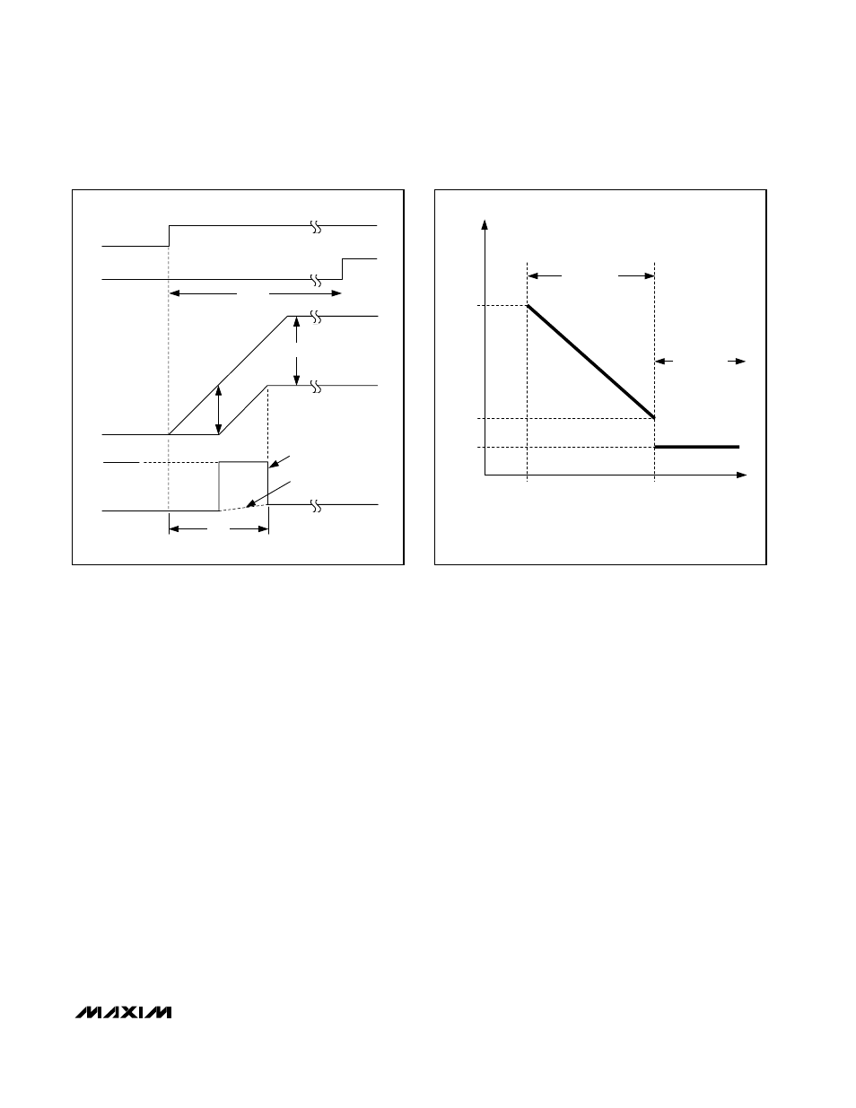
Slow-Comparator Startup Period
The slow comparator is disabled during the startup
period while the external MOSFETs are turning on.
Disabling the slow comparator allows the device to
ignore the higher-than-normal inrush current charging
the board capacitors when a card is first plugged into a
live backplane.
Slow-Comparator Normal Operation
After the startup period is complete, the slow comparator
is enabled and the device enters normal operation. The
comparator threshold voltage (V
SC,TH
) is adjustable from
25mV to 100mV. The slow-comparator response time is
3ms for a 1mV overdrive. The response time decreases
to 100µs with a large overdrive. The variable-speed
response time allows the MAX5927/MAX5929 to ignore
low-amplitude momentary glitches, thus increasing
system noise immunity. After an extended overcurrent
condition, a fault is generated, STAT_ outputs are
deasserted, and the MOSFET gates are discharged with
a 3mA pulldown current.
Fast-Comparator Startup Period
During the startup period, the fast comparator regu-
lates the gate voltages to ensure that the voltage
across the sense resistor does not exceed the startup
fast-comparator threshold voltage (V
SU,TH
), V
SU,TH
is
scaled to two times the slow-comparator threshold
(V
SC,TH
).
Fast-Comparator Normal Operation
In normal operation, if the load current reaches the fast-
comparator threshold, a fault is generated, STAT_ is
deasserted, and the MOSFET gates are discharged
with a strong 50mA pulldown current. This happens in
the event of a serious current overload or a dead short.
The fast-comparator threshold voltage (V
FC,TH
) is
scaled to two times the slow-comparator threshold
(V
SC,TH
). This comparator has a fast response time of
200ns (Figure 7).
Undervoltage Lockout (UVLO)
The UVLO prevents the MAX5927/MAX5929 from turn-
ing on the external MOSFETs until one input voltage
exceeds the UVLO threshold (2.45V) for t
D,UVLO
. The
MAX5927/MAX5929 use power from the highest input
voltage rail for the charge pumps. This allows for more
efficient charge-pump operation. The highest V
IN_
is
provided as an output at BIAS. The UVLO protects the
external MOSFETs from an insufficient gate-drive volt-
MAX5927/MAX5929
Low-Voltage, Quad, Hot-Swap
Controllers/Power Sequencers
______________________________________________________________________________________
15
Figure 6. Independent Mode Startup Waveforms
t
ON
V
DRIVE
V
GATE_
V
GATE_
ON_
STAT_
V
TH
V
OUT_
V
OUT_
I
LOAD_
t
START
C
BOARD_
= LARGE
C
BOARD_
= 0
V
FC,TH
R
SENSE_
Figure 7. VariableSpeed/BiLevel Response
SENSE VOLTAGE (V
IN
- V
SENSE
)
TURN-OFF TIME
V
SC,TH
V
FC,TH
(2 x V
SC,TH
)
3ms
130
µs
200ns
SLOW
COMPARATOR
FAST
COMPARATOR
