Complete, dual, 12-bit multiplying dacs, Detailed description – Rainbow Electronics MX7847 User Manual
Page 6
MX7837/MX7847
_______________Detailed Description
D/A Section
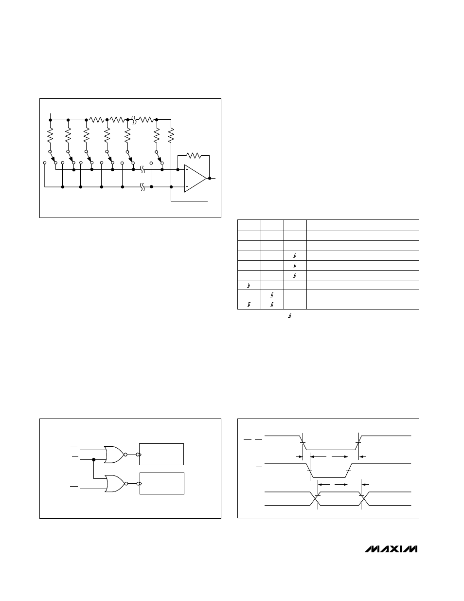
Figure 1 shows a simplified circuit diagram for one of
the DACs and the output amplifier. Using a segmented
scheme, the two MSBs of the 12-bit data word are
decoded to drive the three switches (A to C). The
remaining 10 bits drive the switches (S0 to S9) in a
standard R-2R ladder.
Each switch (A to C) directs 1/4 of the total reference
current, and the remaining current passes through the
R-2R section.
The output amplifier and feedback resistor convert cur-
rent to voltage as follows: V
OUT_
= (-D)(V
REF_
), where D
is the fractional representation of the digital word. (D
can be set from 0 to 4095/4096.)
The output amplifier is capable of developing ±10V
across a 2k
Ω
load. It is internally compensated and
settles to 0.01% FSR (1/2LSB) in less than 4µs. V
OUT
on the MX7837 is not internally connected to R
FB
.
Interface Logic Information
(MX7847)
Figure 2 shows the MX7847 input control logic. The
device contains two independent DACs, each with its
own
CS input and a common WR input. CSA and WR
control data loading to the DAC A latch, and
CSB and
WR control data loading to the DAC B latch. The latch-
es are edge triggered so that input data is latched to
the respective latch on
WR's rising edge. The same
data will be latched to both DACs if
CSA and CSB are
low and
WR is taken high. Table 1 shows the device
control-logic truth table, and Figure 3 shows the write-
cycle timing diagram.
Table 1. MX7847 Truth Table
X = Don't Care
= Rising Edge Triggered
Interface Logic Information
(MX7837)
The MX7837 input loading structure is configured for
interfacing with 8-bit-wide data-bus microprocessors.
Each DAC has two 12-bit latches: an input latch, and a
DAC latch. Each input latch is subdivided into a least-
significant 8-bit latch and a most-significant 4-bit latch.
The data held in the DAC latches determines the out-
puts. Figure 4 shows the MX7837 input control logic,
and Figure 5 shows the write-cycle timing diagram.
Complete, Dual, 12-Bit
Multiplying DACs
6
_______________________________________________________________________________________
2R
2R
2R
2R
2R
2R
2R
C
B
A
S9
S8
S0
V
REF
R
R
R
R/
2
V
OUT
AGND
SHOWN FOR ALL 1s ON DAC
DAC A LATCH
DAC B LATCH
CSA
WR
CSB
Figure 1. D/A Simplified Circuit Diagram
t
3
t
1
t
2
t
5
t
4
VALID DATA
WR
CSA, CSB
DATA
Figure 2. MX7847 Input Control Logic
Figure 3. MX7847 Write-Cycle Timing Diagram
CSA
CSB
WR
Function
X
X
1
No Data Transfer
1
1
X
No Data Transfer
0
1
Data Latched to DAC A
1
0
Data Latched to DAC B
0
0
Data Latched to Both DACs
1
0
Data Latched to DAC A
1
0
Data Latched to DAC B
0
Data Latched to Both DACs