Pin description, Typical operating characteristics (continued) – Rainbow Electronics MX7847 User Manual
Page 5
MX7837/MX7847
Complete, Dual, 12-Bit
Multiplying DACs
_______________________________________________________________________________________
5
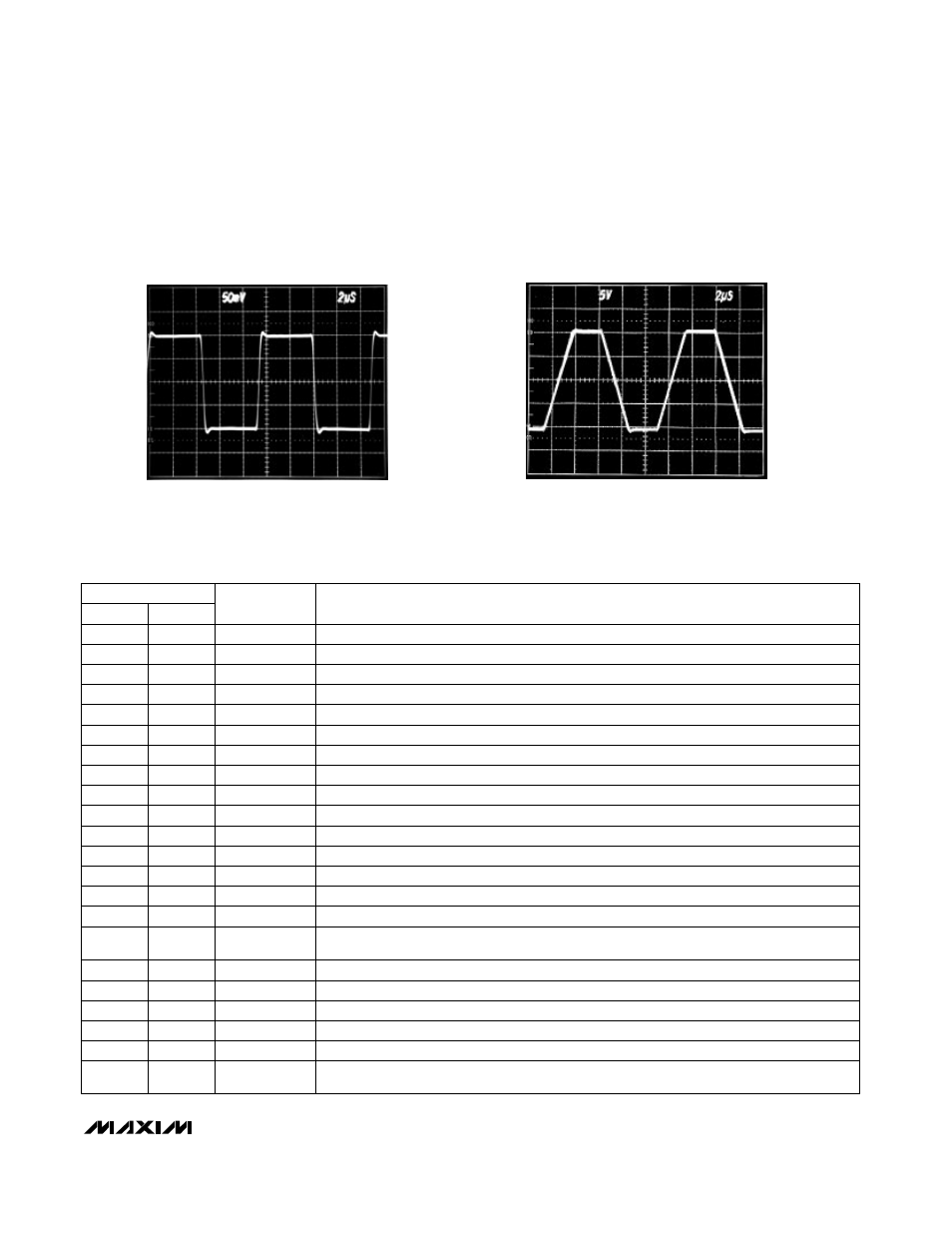
A
AGNDA
A = V
OUTA
, 50mV/div
TIMEBASE = 2
µ
s/div
V
REFA
= ±100mV SQUARE WAVE
SMALL-SIGNAL PULSE RESPONSE
A
AGNDA
A = V
OUTA
, 5V/div
TIMEBASE = 2
µ
s/div
V
REFA
= ±10V SQUARE WAVE
LARGE-SIGNAL PULSE RESPONSE
______________________________________________________________Pin Description
PIN
MX7837
MX7847
NAME
FUNCTION
1
–
CS
Chip Select – active-low logic input
–
1
CSA
Chip-Select Input for DAC A – active-low logic input
2
R
FBA
Amplifier Feedback Resistor for DAC A
–
2
CSB
Chip-Select Input for DAC B – active-low logic input
3
3
V
REFA
Reference Input Voltage for DAC A
4
4
V
OUTA
Analog Output Voltage from DAC A
5
5
AGNDA
Analog Ground for DAC A
6
6
V
DD
Positive Power Supply
–
7
7
V
SS
Negative Power Supply
8
8
AGNDB
Analog Ground for DAC B
9
9
V
OUTB
Analog Output Voltage from DAC B
10
10
V
REFB
Reference Input Voltage for DAC B
11
11
DGND
Digital Ground
12
–
R
FBB
Amplifier Feedback Resistor for DAC B
–
12
DB11
Data Bit 11 (MSB)
13
13
WR
Write Input – active-low logic input (MX7837); positive-edge-triggered input used with
CSA and CSB (MX7847)
14
–
LDAC
Asynchronous Load – DAC input, active-low
–
14-24
DB10-DB0
Data Bit 10 to Data Bit 0 (LSB)
15
–
A1
Address Input – most significant address input for input latches
16
–
A0
Address Input – least significant address input for input latches
17-20
–
DB7-DB4
Data Bit 7 to Data Bit 4
21-24
–
DB3/DB11-
DB0/DB8
Data Bit 3 to Data Bit 0 (LSB), or Data Bit 11 (MSB) to Data Bit 8
____________________________Typical Operating Characteristics (continued)
(T
A
= +25°C, V
DD
= 15V, V
SS
= -15V, R
L
= 2k
Ω
, C
L
= 100pF, unless otherwise noted.)