Pin description, Typical operating characteristics (continued) – Rainbow Electronics MAX5051 User Manual
Page 9
MAX5051
Parallelable, Clamped Two-Switch
Power-Supply Controller IC
_______________________________________________________________________________________
9
Pin Description
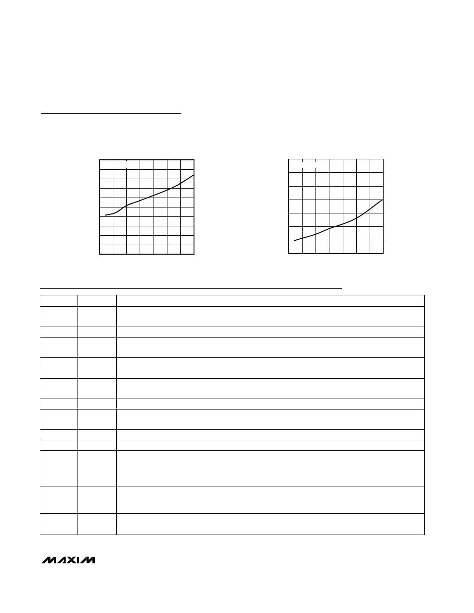
CON TO DRVL PROPAGATION DELAY
vs. TEMPERATURE
MAX5051 toc28
TEMPERATURE (
°C)
PROPAGATION DELAY (ns)
100
75
25
50
0
-25
65
70
75
80
85
90
95
100
105
110
60
-50
125
50mV OVERDRIVE
CS CURRENT LIMIT TO DRVH
PROPAGATION DELAY vs. TEMPERATURE
MAX5051 toc29
TEMPERATURE (
°C)
PROPAGATION DELAY (ns)
100
75
50
25
0
-25
90
100
110
120
130
140
150
80
-50
125
50mV OVERDRIVE
Typical Operating Characteristics (continued)
(V
AVIN
= V
PVIN
= 12V, V
UVLO
= V
STT
= 3V, V
CON
= 3V, R
RCOSC
= 24k
Ω, C
CSS
= 10nF, C
RCOSC
= 100pF, C
REG9
= 4.7µF, C
REG5
=
4.7µF, T
A
= +25°C, unless otherwise noted.)
PIN
NAME
FUNCTION
1
RCOSC
Osci l l ator Fr eq uency S et Inp ut. C onnect a r esi stor fr om RC OS C to RE G5 and a cap aci tor fr om RC OS C to GN D
to set the osci l l ator fr eq uency. S w i tchi ng fr eq uency i s 1/2 the fr eq uency of the saw tooth si g nal at RC OS C .
2
SYNCOUT
Synchronization Output. Synchronization signal to drive SYNCIN of a second MAX5051, if used.
3
RCFF
Feed-Forward Input. Connect a resistor from RCFF to AVIN and a capacitor from RCFF to GND. This is
the PWM ramp.
4
CON
PWM Comparator Noninverting Input. Connect CON to the optocoupler output for isolated applications,
or to COMP for nonisolated applications.
5
CSS
Soft-Start and Reference. Connect a 0.01µF or greater capacitor from CSS to GND. The 1.24V reference
voltage appears across this capacitor.
6
COMP
Internal Error Amplifier Output
7
FB
Feedback Input. Inverting input of the internal error amplifier. The soft-started reference is connected to
the noninverting input of this amplifier.
8
REG5
5V Linear Regulator Output. Bypass REG5 to GND with a 4.7µF ceramic capacitor.
9
REG9
9V Linear Regulator Output. Bypass REG9 to GND with a 4.7µF ceramic capacitor.
10
PVIN
Regulator Voltage Input. Voltage input to the internal 5V and 9V linear regulators. A high-value resistor
connected from the input supply to PVIN provides the necessary current to charge up the startup
capacitor, and the 400µA standby current required by the MAX5051. After startup, the output of a tertiary
winding is used to provide continued bias to the controller.
11
STT
Startup Threshold Input. Leave STT floating for a default startup voltage of 24V at PVIN. STT can be
modified by connecting external resistors. For high accuracy, choose external resistors with 50k
Ω or less
impedance looking back into the divider.
12
LXVDD
Supply Input for the Secondary-Side Synchronous Pulse Transformer or Optocoupler Driver. LXVDD is
normally connected to REG5.