Rainbow Electronics MAX5051 User Manual
Page 13
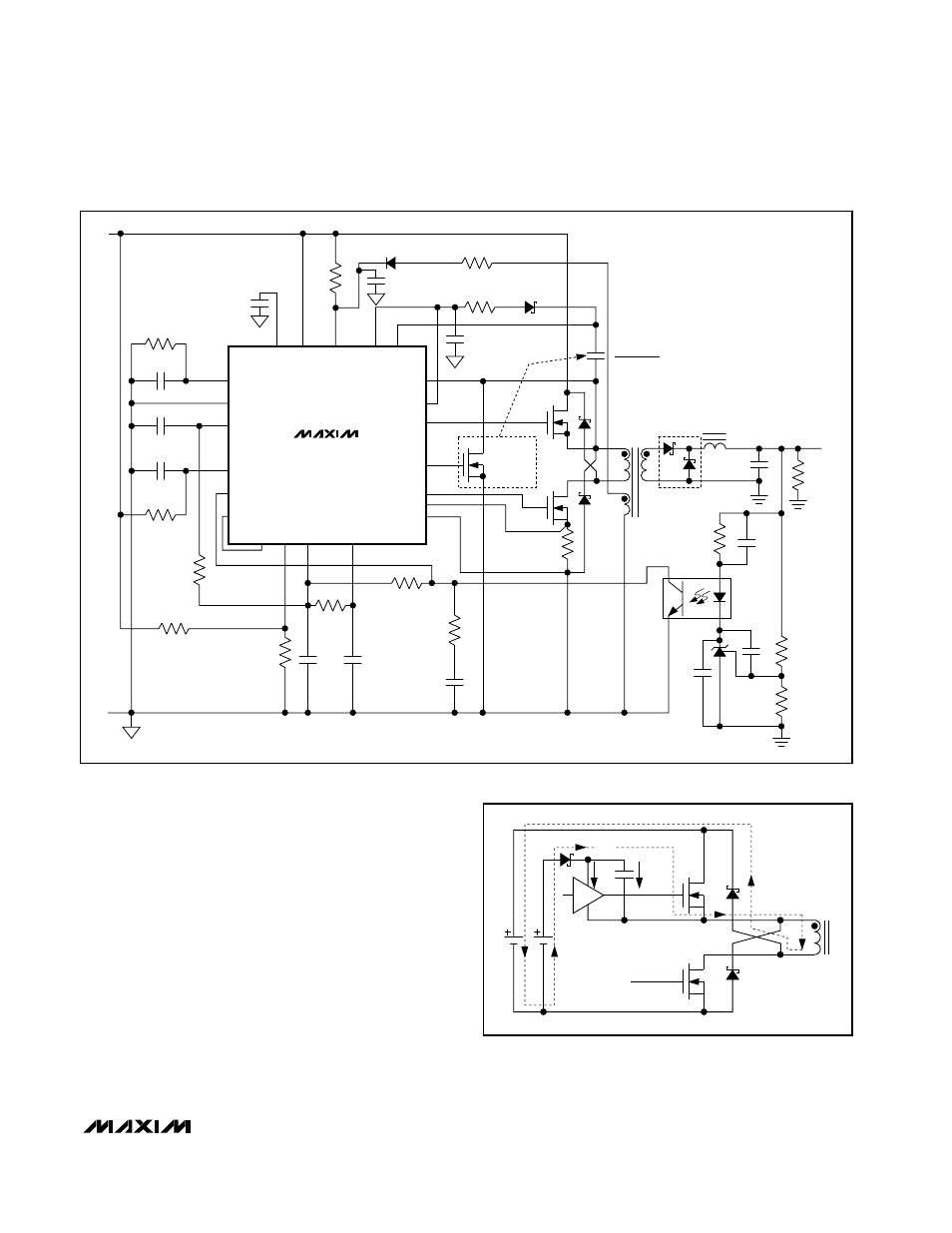
If the charge stored on the boost capacitor is not ade-
quately replenished then the gate-driver lockout for the
high-side MOSFET is triggered, stopping the high side
from switching. The low side continues switching, even-
tually recharging the capacitor, at which point the high
side starts switching again. To prevent this behavior,
use the boost capacitor’s cycle-by-cycle charging cir-
cuit to prevent unwanted shutdowns of the high side
(Figure 2). Connect the gate of a small high-voltage
FET (with the same voltage rating or higher as the main
FETs) to the DRVB output of the MAX5051. Connect the
drain of this FET to XFRMRH, and connect the source
to the primary ground. DRVB will briefly (300ns) turn
this FET ON every cycle after the main PWM clock ter-
minates. This allows the boost capacitor to be replen-
ished under all conditions, even when switching stops
completely. A suitable FET for this is BSS123 or equiva-
lent (100V, 170mA rated). The boost-capacitor charge
MAX5051
Parallelable, Clamped Two-Switch
Power-Supply Controller IC
______________________________________________________________________________________
13
MAX5051
T1
U2
CON
FLTINT
GND
RCFF
RCOSC
STARTUP
FB
BST
REG9
SYNCIN
PVIN
AV
IN
CSS
STT
DRVB
XFRMRH
DRVH
DRVDD
DRVL
PGND
CS
COMP
UVLO
REG5
SYNCOUT
LXVDD
LXH
LXL
V
IN+
3.3V
10A
B2100
T1
L
M
: 150
µH
P: 14T
S: 4T
T: 6T
R
LOAD
MAX8515
USED FOR
BOOST
CAPACITOR
PRECHARGE
PS2913
V
IN-
fs = 250kHz
R12
1M
Ω
C12
220nF
C13
100pF
C14
390pF
R13
100k
Ω
R14
24.9k
Ω
R15
1M
Ω
R11
39.2k
Ω
C10
4.7
µF
C9
1
µF
R10
10
Ω
R8
2.2k
Ω
R7
360
Ω
C6
270nF
R1
11.5k
Ω
R2
2.55k
Ω
C1
47nF
C2
220nF
R3
475
Ω
C3
150nF
C4
3 x 270
µF
L1
2
µH
D5
D2
B2100
D1
N1
SI4486
N2
SI4486
N3
BSS123
R4
28m
Ω
C5
1
µF
C7
4.7
µF
R5
10
Ω
D3
BAT46W
R6
47
Ω
C8
4.7
µF
D4
MA111CT
R9
15k
Ω
C11
0.1
µF
Figure 2. Typical Application Circuit
V
IN
REG9
I
BST
I
BST
L
M
I
GD
I
LM
DRVL
DRVH
XFMRH
BST
Figure 3. Boost Capacitor Charging Path During Transformer
Reset