Rainbow Electronics MAX5051 User Manual
Page 2
MAX5051
Parallelable, Clamped Two-Switch
Power-Supply Controller IC
2
_______________________________________________________________________________________
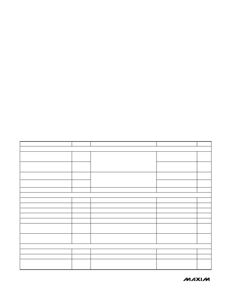
ABSOLUTE MAXIMUM RATINGS
ELECTRICAL CHARACTERISTICS
(AVIN = 12V, PVIN = 12V, V
UVLO
= V
STT
= 3V, V
CON
= 3V, R
RCOSC
= 24k
Ω, C
CSS
= 10nF, C
RCOSC
= 100pF, C
REG9
= 4.7µF,
C
REG5
= 4.7µF, T
A
= T
MIN
to T
MAX
, unless otherwise noted. Typical values are at T
A
= +25°C. All driver, voltage-regulator, and refer-
ence outputs unconnected except for bypass capacitors.)
Stresses beyond those listed under “Absolute Maximum Ratings” may cause permanent damage to the device. These are stress ratings only, and functional
operation of the device at these or any other conditions beyond those indicated in the operational sections of the specifications is not implied. Exposure to
absolute maximum rating conditions for extended periods may affect device reliability.
AVIN, PVIN, XFRMRH to GND................................-0.3V to +80V
BST to GND ............................................................-0.3V to +95V
BST, DRVH to XFRMRH..........................................-0.3V to +12V
REG9, DRVDD, DRVL to GND................................-0.3V to +12V
DRVB, LXVDD, LXL, LXH to GND ..........................-0.3V to +12V
UVLO, STT, COMP, CON to GND ..........................-0.3V to +12V
FLTINT, RCFF to GND ............................................-0.3V to +12V
REG5, CS, CSS, FB to GND .....................................-0.3V to +6V
STARTUP, SYNCIN to GND......................................-0.3V to +6V
SYNCOUT, RCOSC to GND .....................................-0.3V to +6V
PGND to GND .......................................................-0.3V to +0.3V
LXL, LXH Current Continuous...........................................±50mA
DRVL, DRVH Current Continuous...................................±100mA
DRVL, DRVH Peak Current (<500ns) ....................................±5A
PVIN, REG9 Continuous Current ....................................+120mA
REG5 Continuous Current ................................................+80mA
DRVB, RCFF, RCOSC, CSS Continuous Current .............±20mA
COMP, SYNCOUT Continuous Current ............................±20mA
REG9, REG5, and COMP Short to GND ....................Continuous
Continuous Power Dissipation (T
A
= +70°C)
28-Pin TSSOP (derate 23.8mW/°C above +70°C) .....1905mW
28-Pin TSSOP (
θ
JA
)......................................................42°C/W
Operating Temperature Range .........................-40°C to +125°C
Maximum Junction Temperature (T
J
) ..............................+150°C
Storage Temperature Range .............................-65°C to +150°C
Lead Temperature (soldering, 10s) .................................+300°C
PARAMETER
SYMBOL
CONDITIONS
MIN
TYP
MAX
UNITS
SUPPLY CURRENT (AVIN, PVIN)
AVIN Standby Current
I
ASTBY
300
450
µA
PVIN Standby Current
I
PSTBY
V
AVIN
= V
PVIN
= 11V to 76V;
V
STARTUP
= V
CS
= 0V;
V
BST
= V
XFRMRH
= V
DRVDD
= V
REG9
;
RCFF floating
400
650
µA
AVIN Supply Current
I
AVIN
0.65
1
mA
PVIN Supply Current
I
PVIN
V
AVIN
= V
PVIN
= 11V to 76V; V
CS
= 0V;
V
BST
= V
DRVDD
= V
REG9
; V
XFRMRH
= 0V;
STARTUP, RCFF floating
8
12
mA
AVIN Input Voltage Range
Inferred from AVIN supply current test
11
76
V
+9V LDO (REG9)
PVIN Input Voltage Range
V
PVIN
Inferred from PVIN supply current test
11
76
V
REG9 Output-Voltage Set Point
V
REG9
V
PVIN
= 11V
8.3
9.0
V
REG9 Line Regulation
V
PVIN
= 11V to 76V
0.1
mV/V
REG9 Load Regulation
I
REG9
= 0 to 80mA
250
mV
REG9 Dropout Voltage
I
REG9
= 80mA
0.5
V
REG9 Undervoltage Lockout
Threshold
V
REG9
falling
5.7
6.7
V
REG9 Undervoltage Lockout
Threshold Hysteresis
750
mV
+5V LDO (REG5)
REG5 Output-Voltage Set Point
V
REG5
4.8
5.1
V
REG5 Load Regulation
I
REG5
= 0 to 40mA
50
mV
REG5 Dropout Voltage
I
REG5
= 40mA, measured with respect
to V
REG9
0.5
V