C-compatible serial interface in a sot23, Detailed description – Rainbow Electronics MAX6626 User Manual
Page 5
MAX6625/MAX6626
9-Bit/12-Bit Temperature Sensors with
I
2
C-Compatible Serial Interface in a SOT23
_______________________________________________________________________________________
5
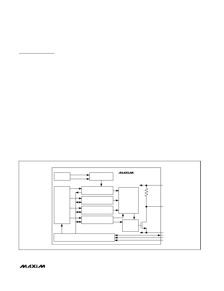
Detailed Description
The MAX6625/MAX6626 continuously convert their die
temperatures into digital values using their self-con-
tained delta-sigma ADCs. The resulting data is read-
able at any time through the I
2
C-compatible serial
interface. A dedicated alarm output asserts if the result
exceeds the value in the programmable high-tempera-
ture register. A programmable fault queue sets the
number of faults that must occur before the alarm
asserts, preventing spurious alarms in noisy environ-
ments. The alarm output polarity is selectable and
deasserts based on either of two operating modes,
comparator or interrupt. In comparator mode, the OT
output deasserts if the temperature conversion result
falls below the programmable low-temperature register
value (subject to the fault queue conditions) providing
adjustable hysteresis. In interrupt mode, the OT output
deasserts when any register is read through the serial
interface. Each conversion cycle takes about 130ms. At
power-up, the temperature register is set to 8000H until
the first conversion is completed.
The MAX6625/MAX6626 feature a shutdown mode,
accessible through the serial interface, that saves power
by turning off everything but the power-on reset and the
I
2
C-compatible interface. While in shutdown mode the
temperature register is set to 8000H. The device func-
tions as a slave on the I
2
C-compatible bus supporting
Write Byte, Write Word, Read Byte, and Read Word com-
mands. Four separate addresses can be configured with
the ADD pin, allowing up to four MAX6625/MAX6626
devices to be placed on the same bus. Figure 2 shows
the functional block diagram of the MAX6625/MAX6626.
Serial interface
I
2
C-Compatible Operation
The MAX6625/MAX6626 are readable and programma-
ble through their I
2
C-compatible serial interface.
Figures 3 and 4 show the timing details of the clock
(SCL) and data (SDA) signals. The device functions as
a slave on the I
2
C-compatible bus and supports Write
Byte, Write Word, Read Byte, and Read Word com-
mands.
Addressing
Four separate addresses can be configured with the
ADD pin, allowing up to four MAX6625/MAX6626s to be
placed on the same bus. The address is selected by
connecting the ADD pin to either of four places: GND
(address 0), V
S
(address 1), SDA (address 2), or SCL
(address 3). Table 1 shows the full I
2
C-compatible
address for each state.
MAX6625
MAX6626
TEMPERATURE REGISTER
T
HIGH
REGISTER
+Vs
OT
GND
SDA
SCL
ADD
SERIAL BUS INTERFACE
T
LOW
REGISTER
SET-POINT
COMPARATOR
ADDRESS
POINTER
REGISTER
BANDGAP
REGISTER
ADC
REFERENCE
TEMP SIGNAL
FAULT
QUEUE
COUNTER
CONFIGURATION REGISTER
MAX665_ R
ONLY
Figure 2. Functional Block Diagram