Table 1. temperature data byte format – Rainbow Electronics MAX6678 User Manual
Page 7
The DXN input is biased at 0.60V above ground by an
internal diode to set up the analog-to-digital inputs for a
differential measurement. The worst case DXP-DXN dif-
ferential input voltage range is from 0.25V to 0.95V.
Excess resistance in series with the remote diode causes
about +0.5°C error per ohm. Likewise, a 200µV offset
voltage forced on DXP-DXN causes about 1°C error.
High-frequency EMI is best filtered at DXP and DXN with
an external 2200pF capacitor. This value can be
increased to about 3300pF (max), including cable capac-
itance. Capacitance higher than 3300pF introduces
errors due to the rise time of the switched current source.
MAX6678
2-Channel Temperature Monitor with Dual Automatic
PWM Fan-Speed Controller and Five GPIOs
_______________________________________________________________________________________
7
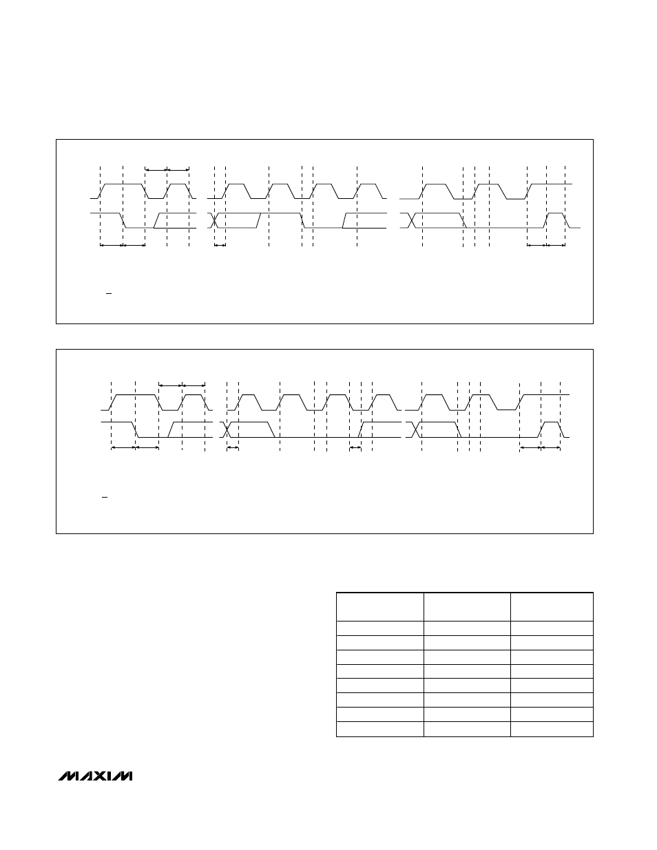
SMBCLK
A = START CONDITION
B = MSB OF ADDRESS CLOCKED INTO SLAVE
C = LSB OF ADDRESS CLOCKED INTO SLAVE
D = R/W BIT CLOCKED INTO SLAVE
A
B
C
D
E
F
G
H
I
J
SMBDATA
t
SU:STA
t
HD:STA
t
LOW
t
HIGH
t
SU:DAT
t
SU:STO
t
BUF
L
M
K
E = SLAVE PULLS SMBDATA LINE LOW
F = ACKNOWLEDGE BIT CLOCKED INTO MASTER
G = MSB OF DATA CLOCKED INTO SLAVE
H = LSB OF DATA CLOCKED INTO SLAVE
I = MASTER PULLS DATA LINE LOW
J = ACKNOWLEDGE CLOCKED INTO SLAVE
K = ACKNOWLEDGE CLOCK PULSE
L = STOP CONDITION
M = NEW START CONDITION
Figure 2. SMBus Write Timing Diagram
SMBCLK
A
B
C
D
E
F
G
H
I
J
K
SMBDATA
t
SU:STA
t
HD:STA
t
LOW
t
HIGH
t
SU:DAT
t
HD:DAT
t
SU:STO
t
BUF
A = START CONDITION
B = MSB OF ADDRESS CLOCKED INTO SLAVE
C = LSB OF ADDRESS CLOCKED INTO SLAVE
D = R/W BIT CLOCKED INTO SLAVE
E = SLAVE PULLS SMBDATA LINE LOW
L
M
F = ACKNOWLEDGE BIT CLOCKED INTO MASTER
G = MSB OF DATA CLOCKED INTO MASTER
H = LSB OF DATA CLOCKED INTO MASTER
I = MASTER PULLS DATA LINE LOW
J = ACKNOWLEDGE CLOCKED INTO SLAVE
K = ACKNOWLEDGE CLOCK PULSE
L = STOP CONDITION
M = NEW START CONDITION
Figure 3. SMBus Read Timing Diagram
Table 1. Temperature Data Byte Format
TEMP (°C)
ROUNDED TEMP
(°C)
DIGITAL OUTPUT
241
+241
1111 0001
240
+240
1111 0000
126
+126
0111 1110
25
+25
0001 1001
0.50
+1
0000 0001
0.00
0
0000 0000
Diode fault (open)
—
1110 1111
Diode fault (short)
—
1111 1111