10ria series, Blocking, Triggering – C&H Technology 10RIA Series User Manual
Page 4: Switching
10RIA Series
Bulletin I2405 rev. B 04/06
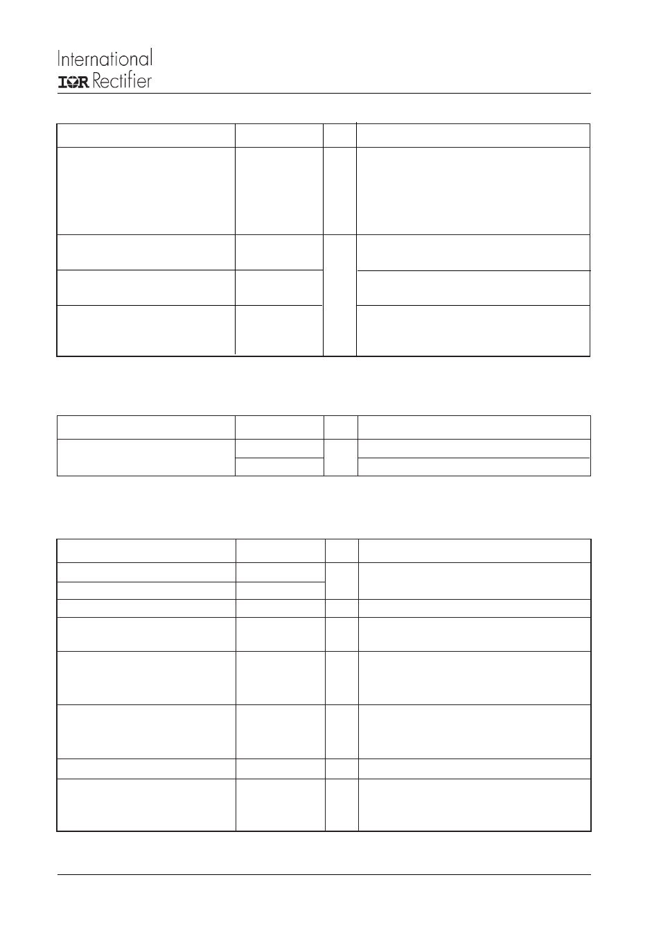
dv/dt
Max. critical rate of rise of
100
T
J
= T
J
max. linear to 100% rated V
DRM
off-state voltage
300 (*)
T
J
= T
J
max. linear to 67% rated V
DRM
V/μs
Parameter
10RIA
Units Conditions
Blocking
P
GM
Maximum peak gate power
8.0
T
J
= T
J
max.
P
G(AV)
Maximum average gate power
2.0
I
GM
Max. peak positive gate current
1.5
A
T
J
= T
J
max.
-V
GM
Maximum peak negative
10
V
T
J
= T
J
max.
gate voltage
I
GT
DC gate current required
90
T
J
= - 65°C
to trigger
60
mA
T
J
= 25°C
35
T
J
= 125°C
V
GT
DC gate voltage required
3.0
T
J
= - 65°C
to trigger
2.0
V
T
J
= 25°C
1.0
V
T
J
= 125°C
I
GD
DC gate current not to trigger
2.0
mA
T
J
= T
J
max., V
DRM
= rated value
V
GD
DC gate voltage not to trigger
0.2
V
T
J
= T
J
max.
V
DRM
= rated value
W
Max. required gate trigger current/
voltage are the lowest value which
will trigger all units 6V anode-to-
cathode applied
Max. gate current/ voltage not to
trigger is the max. value which
will not trigger any unit with rated
V
DRM
anode-to-cathode applied
Parameter
10RIA
Units Conditions
Triggering
di/dt
Max. rate of rise of turned-on
T
J
= T
J
max., V
DM
= rated V
DRM
current
V
DRM
≤ 600V
200
A/μs
Gate pulse = 20V, 15
Ω, t
p
= 6μs, t
r
= 0.1μs max.
V
DRM
≤ 800V
180
I
TM
= (2x rated di/dt) A
V
DRM
≤ 1000V
160
V
DRM
≤ 1600V
150
t
gt
Typical turn-on time
0.9
T
J
= 25°C,
at = rated V
DRM
/V
RRM
, T
J
= 125°C
t
rr
Typical reverse recovery time
4
μs
T
J
= T
J
max.,
I
TM
= I
T(AV)
, t
p
> 200μs, di/dt = -10A/μs
t
q
Typical turn-off time
110
T
J
= T
J
max., I
TM
= I
T(AV)
, t
p
> 200μs,
V
R
= 100V,
di/dt = -10A/μs, dv/dt = 20V/μs linear to
67% V
DRM
, gate bias 0V-100W
Parameter
10RIA
Units Conditions
Switching
(**) Available with: dv/dt = 1000V/μs, to complete code add S90 i.e. 10RIA120S90.
(*) t
q
= 10μsup to 600V, t
q
= 30μs up to 1600V available on special request.
Document Number: 93689
www.vishay.com
3