Electrical and mechanical characteristics, t, 25°c unless otherwise specified inverter sector, Thermal and mechanical characteristics, t – C&H Technology CM150RX-12A User Manual
Page 4: 25°c unless otherwise specified
CM150RX-12A
Six IGBTMOD™ + Brake NX-Series Module
150 Amperes/600 Volts
Powerex, Inc., 173 Pavilion Lane, Youngwood, Pennsylvania 15697 (724) 925-7272
3
Rev. 11/08
Electrical and Mechanical Characteristics,
T
j
= 25°C unless otherwise specified
Inverter Sector
Characteristics
Symbol
Test Conditions
Min.
Typ.
Max.
Units
Collector Cutoff Current
I
CES
V
CE
= V
CES
, V
GE
= 0V
—
—
1.0
mA
Gate-Emitter Threshold Voltage
V
GE(th)
I
C
= 15mA, V
CE
= 10V
5
6
7
Volts
Gate Leakage Current
I
GES
V
GE
= V
GES
, V
CE
= 0V
—
—
0.5
µA
Collector-Emitter Saturation Voltage
V
CE(sat)
I
C
= 150A, V
GE
= 15V, T
j
= 25°C
—
1.7
2.1
Volts
I
C
= 150A, V
GE
= 15V, T
j
= 125°C
—
1.9
—
Volts
I
C
= 150A, V
GE
= 15V, Chip
—
1.6
—
Volts
Input Capacitance
C
ies
— — 18.0 nF
Output Capacitance
C
oes
V
CE
= 10V, V
GE
= 0V
—
—
2.0
nF
Reverse Transfer Capacitance
C
res
— — 0.6 nF
Total Gate Charge
Q
G
V
CC
= 300V, I
C
= 150A, V
GE
= 15V
—
400
—
nC
Inductive
Turn-on Delay Time
t
d(on)
— — 120 ns
Load
Turn-on Rise Time
t
r
V
CC
= 300V, I
C
= 150A,
—
—
100
ns
Switch
Turn-off Delay Time
t
d(off)
V
GE
= ±15V,
— — 350 ns
Time
Turn-off Fall Time
t
f
R
G
= 6.2Ω, I
E
= 150A,
—
—
600
ns
Reverse Recovery Time*
t
rr
Inductive Load Switching Operation
—
—
200
ns
Reverse Recovery Charge*
Qrr
—
5.0
—
µC
Emitter-Collector Voltage*
V
EC
I
E
= 150A, V
GE
= 0V, T
j
= 25°C
—
2.0
2.8
Volts
I
E
= 150A, V
GE
= 0V, T
j
= 125°C
—
1.95
—
Volts
I
E
= 150A, V
GE
= 0V, Chip
—
1.9
—
Volts
Thermal and Mechanical Characteristics,
T
j
= 25°C unless otherwise specified
Characteristics
Symbol
Test Conditions
Min.
Typ.
Max.
Units
Thermal Resistance, Junction to Case**
R
th(j-c)
Q
Per IGBT
—
—
0.24
°C/W
Thermal Resistance, Junction to Case**
R
th(j-c)
D
Per FWDi
—
—
0.46
°C/W
Contact Thermal Resistance**
R
th(c-f)
Thermal
Grease
Applied
— 0.015 — °C/W
Internal Gate Resistance
R
Gint
T
C
= 25°C
—
0
—
Ω
External Gate Resistance
R
G
4.1 — 41 Ω
*Represents characteristics of the anti-parallel, emitter-to-collector free-wheel diode (FWDi).
**T
C
, T
f
measured point is just under the chips.
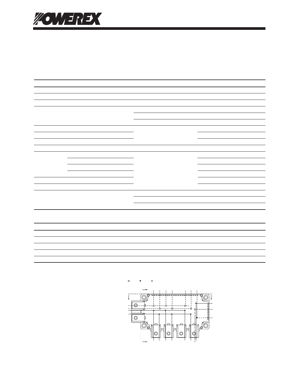
34
20.6
0
0
22.6
34.1
45.3
55.8
79.6
89.3
99.7
0
23.1
33.6
44.8
55.3
79.1
89.6
96.4
97
.8
0
17.3
26.8
41.4
26.0
29.4
35.4
33 32 31 30 29 28 27 26 25 24 23 22
Dimensions in mm (Tolerance: ±1mm)
21 20 19 18 17 16 15 14 13
12
35
36
1
2
3
4
11
10
9
8
7
6
5
IGBT FWDi NTC Thermistor
Chip Location (Top View)
U
P
V
P
W
P
W
N
V
N
U
N
U
P
V
P
W
P
W
N
Br
Th
Br
V
N
U
N
CHIP LOCATION (TOP VIEW)